Engineered materials boost modulator performance
Collaborative research between industry and academia accelerates the development of high-performance, low-voltage waveguide modulators based on the newest technologies.
Jane Zucker
When it comes to modulators, the choice of device material is all-important. Smaller and faster devices rely on large nonlinear effects to yield top performance. From elemental semiconductors to III-V compounds, from homostructure to heterostructure, the advances of the past three decades of optoelectronics technology have been large: extremely sophisticated modulators with quaternary composition, built-in strain, ultrathin quantum wells, and integrated lasers are now routinely manufactured in factories all over the world.
Still, the demand for smaller, faster, and more-efficient devices is growing at increasing speed and with no end in sight. So what is next? Engineered materials, specially designed with supersized optical properties, will form the basis for the next generation of photonic devices. These will include microcavities, quantum dots and wires, and even materials that assemble themselves. Such advances will move communications technology beyond the 40-Gbit/s speeds of today's state-of-the-art electro-optic modulators to an ultrafast all-optical regime for data transmission.
Building modulating materials
To modulate light and to impress signals and data on it, photons somehow must be agitated. The traditional approach to modulation is indirect: alter the properties of an optical medium, then pass light through it. Popular ways for perturbing optical materials include injection of current or application of voltage.
What if the properties of the light could be altered directly? Direct action on the photon could create much stronger optical effects with less dissipation of energy.
FIGURE 1. Scanning electron micrograph shows a gallium arsenide air-bridge microcavity forming a one-dimensional photonic crystal defined by a series of eight regular holes (top). By increasing the distance between two of the holes in the center of the array, a defect is created that gives rise to a sharp peak in optical transmission (bottom).
Nanotechnology is one approach to the direct control of light. In this field of research, tiny chambers are engineered to trap and bounce light waves in a highly regular and resonant way. Such research is under way in a collaboration between Nanovation Technologies (Miami, FL) and the Massachusetts Institute of Technology (MIT) Microphotonics Center (Cambridge, MA), an industrially sponsored, academic-centered research center. There, a group of scientists with backgrounds in chemistry, physics, electrical engineering, and materials science is approaching nanotechnology from multiple angles. For example, MIT chemist Timothy Swager builds devices from the ground up that contain a superstructure composed of designer molecules of precise length, shape, and optical properties, while materials scientist Leslie Kolodziejski engineers a semiconductor structure and then selectively demolishes it, leaving behind a precisely ordered framework.
Photonic bandgap materials
A device structure fabricated by Kolodziejski's group contains an air-bridge microcavity (see Fig. 1).1 The microcavity has the smallest modal volume ever demonstrated, with its finest feature size on the order of 0.2 µm. The suspended gallium arsenide (GaAs) air bridge was formed by electron-beam lithography, followed by a sacrificial etch of the aluminum oxide beneath.
This structure has significance for optical communications. Measured transmission through the microcavity reveals the influence of the photonic bandgap (PBG) structure: a resonance in the 1500-nm wavelength range, a region of the spectrum important to today's fiberoptic transmission systems. The repetitive structure of the microcavity forces photons to follow fixed rules similar to those found in solid-state crystals, where symmetry and regular structure determine the allowed states for electrons. Originally designed by a group led by PBG pioneer John Joannopoulos, the microcavity is precisely engineered to select its resonant wavelength.
Ongoing work is aimed at more-advanced structures for controlling and manipulating these sharp optical features to provide optical modulation, wavelength filtering, and switching. In one modulation scheme, integrated microelectromechanical structures trim the microcavity and tune its resonances in a scaled-down analogy to the movable metallic tuning stubs in microwave waveguides.
Low cost, low loss
Low cost and low loss are probably the most often requested specifications for external optical modulators. Drastic cost reductions in photonic components permit high-bandwidth optics to penetrate further and further into the everyday life of even the most casual Internet user. For example, deployment of local fiber access would be unthinkable without the development of low-cost automated and mass-produced silica and semiconductor components.
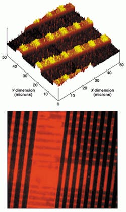
FIGURE 2. Patterned organic thin films contain complex three-dimensional structures at micron-level sizes. An atomic-force-microscope image shows a first-level pattern formed by the selective adsorption of polyelectrolytes on a self-assembled monolayer and a microcontact-printed second-level pattern seen as raised squares (top). The individual stripes are 3.5 µm wide. A fluorescent micrograph reveals dye used in the second-level assembly (bottom).
Nevertheless, the equipment necessary for the fabrication and patterning of these conventional materials is still quite expensive. One cost-effective alternative that is being explored by MIT researcher Edwin Thomas is the manufacture of photonic materials via synthesis of self-assembling block copolymers.2 As the name suggests, the polymers arrange themselves in regular three-dimensional periodic arrays. The equilibrium structure, with length scales of the order of 100 to 1000 Å, results from a delicate balance of forces between different polymer chains that prefer to remain separate yet are weakly bonded together. The polymer ingredients are inexpensive and the actual mixing process is uncomplicated; however, the recipes must be exact and the solutions ultrapure to achieve the desired optical and electrical properties.
Swager, Yoel Fink, and Thomas at MIT are pursuing PBG materials based on block copolymers. In one application, the periodic structure contains a specially engineered filler. The chemical composition of the structure and of the filler can be tailored individually for light-by-light control. For example, if the filler that absorbs radiation is in one region of the spectrum while the cavity modulates radiation at another wavelength, strong modulation with low loss can be obtained.
Another approach to low-cost ordered materials with high dielectric contrast is microprinting, a project pursued by a group led by Paula Hammond at the MIT chemical engineering department. Using a stamp, micron-sized patterns are deposited and then built up in three dimensions using the material's electrical properties (see Fig. 2).
Useful in some electrical and optical devices, such patterns can be made following a technique called self-assembled-monolayer-templated ionic multilayer assembly; in addition, research has also begun into chemically templated patterning. The MIT group has recently adapted commercially available machinery to automate the deposition process.
When will the future become the present?
Commercialization of some of the material approaches under development could be feasible in as little as 18 months, provided the end result yields significant cost savings or system benefits. However, most new material approaches will require three to five years of additional research and development before they are ready for application to commercial markets.
Still, high demand is a powerful force. In the communications field, product life cycles are becoming shorter and shorter. For optical-components manufacturers to maintain their competitive edge, a strong coupling to research and development is essential. One of the strengths of the collaboration between MIT and Nanovation is the two-way interaction between academics and industry. This arrangement provides some commercial focus to fundamental research, offering researchers a ready market for their most-promising projects and providing component manufacturers and their customers with improved technology.
REFERENCES
- D. J. Ripin et al., IEEE J. Lightwave Technology 17(11), 2152 (1999).
- E. L. Thomas, Science, 286, 1307 (1999).
JANE ZUCKER is marketing director for advanced technologies at Nanovation Technologies, 2665 South Bayshore Drive, Ste. 501, Miami, FL 33133; e-mail: [email protected].