Optothermoplasmonic nanolithography patterns 2D materials on demand
Researchers at the University of Texas at Austin have developed an all-optical technique based on plasmon-enhanced optothermal effects for on-demand patterning of atomically thin two-dimensional (2D) materials. Unlike expensive and complex photolithography, electron- and ion-beam lithography, and even high-power femtosecond laser patterning, optothermoplasmonic nanolithography (OTNL) is a low-power, submicron, maskless, and high-throughput process whereby graphene, molybdenum sulfide (MoS2), or other 2D materials are transferred onto a thermoplasmonic substrate (such as a porous gold substrate).
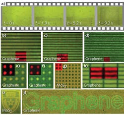
When illuminated by a focused 532 nm laser beam, localized surface-plasmon resonances are excited on the gold thermoplasmonic substrate, inducing well-confined, localized thermal hotspots that can reach a maximum temperature of 850 K when heated by a laser with optical intensity of 6.4 mW/µm2. Dynamic interaction between the thermal hot spots and the 2D materials are further achieved by steering the laser beam through a spatial light modulator (SLM) or with a translation stage.
These hotspots ablate or displace the 2D material through sublimation or other material-dependent mechanisms, creating an array of versatile patterns at submicron resolution. For example, 40 × 40 µm nanoribbon structures on graphene have a 600 nm linewidth and 2 µm periodicity, nanohole arrays on MoS2 have a diameter of 1.1 µm, and the word “graphene” patterned on a graphene substrate has a linewidth of 1.5 µm. Reference: L. Lin et al., Adv. Funct. Mater., 1803990 (Aug. 12, 2018); https://onlinelibrary.wiley.com/doi/abs/10.1002/adfm.201803990.
About the Author

Gail Overton
Senior Editor (2004-2020)
Gail has more than 30 years of engineering, marketing, product management, and editorial experience in the photonics and optical communications industry. Before joining the staff at Laser Focus World in 2004, she held many product management and product marketing roles in the fiber-optics industry, most notably at Hughes (El Segundo, CA), GTE Labs (Waltham, MA), Corning (Corning, NY), Photon Kinetics (Beaverton, OR), and Newport Corporation (Irvine, CA). During her marketing career, Gail published articles in WDM Solutions and Sensors magazine and traveled internationally to conduct product and sales training. Gail received her BS degree in physics, with an emphasis in optics, from San Diego State University in San Diego, CA in May 1986.