ORGANIC OPTOELECTRONICS: European team characterizes photonic-feedback structures for mini organic lasers
A team of researchers from AMO (Aachen, Germany), IBM Research (Rüschlikon, Switzerland), and the University of Wuppertal (Wuppertal, Germany) recently investigated the combination of mixed-order two-dimensional (2-D) photonic-crystal-laser structures with a high-gain organic polymer to tap into its potential for producing a lower lasing threshold and a device-shrinking footprint. They discovered that this combination does indeed produce the desired results.
Organic semiconductor materials have attracted plenty of attention in recent years, thanks to their excellent optical properties and potential use in applications such as displays, sensing, and solar cells. And as Moore’s Law—which states that the number of transistors that can be placed on an integrated circuit (IC) increases exponentially, doubling roughly every two years—reaches its physical limits, combining organic semiconductor materials with optoelectronics could help maneuver around future scaling problems.
A primary goal of this research, which is ongoing, is to take optics closer to the processor by using a CMOS-compatible material to work around Moore’s Law. “If we can use already existing CMOS technology, it cuts down on costs,” explains Rainer Mahrt, a research member of IBM Research’s Exploratory Photonics Team. “That’s why we selected an organic polymer as our gain material, as well as tantalum pentoxide (Ta2O5) for the photonic-crystal layer. The optical properties of the gain material are simple to adjust by modifying the polymer backbone and/or the side-groups, allowing adjustment of the emission at the desired wavelength. Furthermore, Ta2O5 is an amorphous material with a high refractive index. It is transparent in the wavelength range we’re interested in lasing at and enhances the optical feedback. Tantalum pentoxide is also CMOS-compatible and easy to handle.”
Mitigating light loss
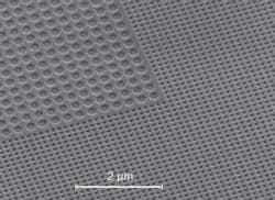
One drawback of this design, Mahrt says, is that in the 2-D, second-order photonic crystal structure, light is simply lost at the edge of the feedback structure. To overcome this loss of light, the researchers surrounded the second-order structure with a first-order photonic-crystal structure to act as a nearly perfect mirror (see figure). This confines more light within the resonator and results in a much smaller footprint of the lasing device. “We confine the light not only in one direction, but two—within the plane of the device structure,” says Mahrt. “This leads to an output coupling that is more or less circular shaped.”
The team reports that laser structures were then fabricated on a silicon substrate with 1.8 µm of thermal oxide.1 A 30-nm-thick layer of Ta2O5 was deposited in a reactive-sputter deposition process, with a refractive index of n = 2.16 at the wavelength of 500 nm, as measured by spectroscopic ellipsometry. Electron-beam lithography was used next, followed by a transfer of the resist pattern to the Ta2O5 layer with an SF6/C4F8-based reactive-ion etching process. The resulting mixed first- and second-order photonic feedback structures consisted of a square lattice of holes with diameters of 100 and 150 nm pitch and holes with diameters of 213 and 300 nm pitch. This increased both the index contrast between the gain material and photonic crystal, as well as the optical confinement, according to the researchers.
When it began this project, the team wanted to extend the wavelengths of the laser sources into the visible-to generate higher bandwidth. “A challenge for semiconductor materials is that not many show lasing in the visible,” Mahrt notes. “There’s gallium nitride (GaN) on one hand, which is around 400 nm. The next is around 630 nm. To my knowledge, until now, there was no material between them that could be easily prepared and structured in the visible wavelength range. So we’ve jumped into the field of organic materials. Our group and others have shown that this particular polymer material—ladder-type poly(p-phenylene)—provides a huge optical gain of about 2000 cm-1, which is rather high compared to other materials. And because it’s a polymer, you can spin-coat it onto a substrate easily, which is highly desirable.”
Organic lasers with small-footprint structures may also provide an appealing packaging possibility for light-emitting arrays coupled to high-density optical interconnects. And the researchers believe they can further optimize the device, for example, the distance between the first- and second-order photonic-crystal structures, to suppress destructive interference effects—meaning there’s room for improvement in terms of achieving an even lower threshold and smaller footprint for the device.
REFERENCE
1. K. Baumann et al., Appl. Phys. Lett.91, 171108 (2007).
About the Author
Sally Cole Johnson
Editor in Chief
Sally Cole Johnson, Laser Focus World’s editor in chief, is a science and technology journalist who specializes in physics and semiconductors.

