SILICON PHOTONICS: Silicon lasers push into the mid-IR
The mid-infrared portion of the electromagnetic spectrum is generally a hard one to reach with laser sources, typically involving large and complex setups. Soon, however, tiny silicon lasers might cover the range with the smallest, simplest approach yet.
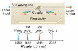
Haisheng Rong and colleagues at Intel (Santa Clara, CA, and Jerusalem, Israel) have demonstrated the first “cascaded Raman” laser in silicon. The idea—first suggested in several modeling approaches in 2006 and 2007—is that in an appropriately structured silicon microcavity, pump light can undergo multiple Stokes shifts, resulting in mid-IR output.
Ozdal Boyraz, an electrical engineer from the University of California at Irvine, demonstrated the first silicon-based Raman laser in 2004.1 “Raman is a splendid tool to shift the frequency of an existing laser,” Boyraz says. “The process is wavelength independent and the amount of frequency shift is determined by phonon oscillations. Hence, a frequency down-converted pump signal can act as a pump of a second frequency down-conversion.”
Boyraz’s work showed the first-order Raman peak in silicon, at 1675 nm. However, the process can continue cascading, with each new order further into the infrared (see Fig. 1). Similar cascaded Raman effects have been shown in silica fibers and microcavities, but silica experiences high losses in the mid-IR. Silicon, on the other hand, shows a high Raman gain and optical transparency well into the mid-IR (see www.laserfocusworld.com/articles/248133).Spectral purity
Mario Paniccia, director of Intel’s Photonics Technology Lab and senior author on the research, has been pushing toward the result for some time. “This program started when we were working on optical testing of microprocessors. We couldn’t understand why the components were so expensive, so we aimed to build the optical devices in silicon,” Paniccia says. “Along the way, we started looking at this Raman effect and thought that if we could get that going, we could get gain.”
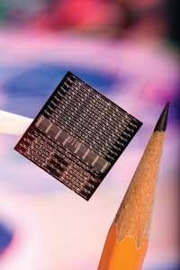
The team used a silicon-on-insulator waveguide in a “racetrack” cavity with a total length of 3 cm (see Fig. 2). Pumping with light around 1550 nm, the output Raman lines were at 1686 and 1848 nm, with as much as 5 mW output in the second-order peak. Tuning was accomplished simply by tuning the pump wavelength while temperature-tuning the cavity resonance to match. The free-carrier absorption, which would otherwise drastically reduce the Raman gain in the cavity, was mitigated by forming a p-i-n diode structure on either side of the waveguide. By biasing it at 25 V the free-carrier absorption was reduced by more than 35 times.2
Paniccia says he was surprised by just how well the approach worked. “The spectral purity and stability of these things are amazing,” he says. In particular, he cites the narrow linewidth of the emission, which he says is actually below their measurement threshold. To show its lasers in a gas sensing application, the team measured the absorption spectrum of a water/methane sample. “The resolution of that measurement is so high that you can actually see the effects of the molecular orbitals of methane,” Paniccia says.
Potential applications
Boyraz is impressed with the outcome. “The most compelling result coming of this research is the prospect of having high-power mid-IR lasers operating at room temperature at any wavelength between 2.5 and 7 µm,” he says. But he warns that the jump from the current result to that kind of flexibility is not an easy one. “Starting from a telecom wavelength to reach mid-IR wavelengths is a challenge. At every step of frequency shift, the Raman effect has to compete with nonlinear losses such as degenerate and nondegenerate two-photon absorption, and associated free-carrier absorption.” Boyraz suggests an approach that starts around 2 µm, because the nonlinear losses drop several orders of magnitude beyond that point.
The small form factor and low threshold will make the devices ideal for minuscule sensors, perhaps combined with wireless transmitters for industrial applications. Paniccia says the next step is to design tunable couplers for wider ranges of wavelengths—making for quite possibly the smallest IR spectrometers ever. Even in its current form, Intel recognizes the potential of the technology, with interest from its biosciences and health arms.
REFERENCES
1. O. Boyraz and B. Jalali, Opt. Express 12, 5269 (2004).
2. Rong et al., Nature Photonics, DOI: 10.1038/nphoton.2008.

