NANOPHOTONICS: Near-field polishing yields ultraflat silica surface
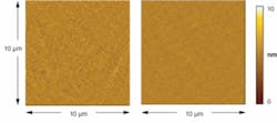
Conventional chemical-mechanical polishing (CMP) methods are typically used to obtain surfaces figured to sub-100-nm tolerances on optical and semiconductor materials for specialized applications. While CMP methods can yield surface roughnesses on fused silica down to approximately 2.36 Å, scientists at the Japan Science and Technology Agency (SORST), the University of Tokyo, and Sigma Koki (all in Tokyo, Japan) have developed an optical near-field, nonadiabatic photochemical photodissociation process that can further polish this type of surface to a roughness of only 1.37 Å.1
Photodissociation is the process by which light energy causes reacting molecular gases to resonate in order to excite molecules from the ground state to an excited electronic state. The near-field polishing process uses light at a 532 nm wavelength from a continuous-wave laser in the presence of molecular chlorine (Cl2), which serves as an etching gas; the laser light selectively photodissociates the chlorine near surface protrusions on the silica substrate.
Because the photon energy of the 523 nm light is lower than the absorption-band energy of the chlorine molecule (400 nm), conventional photo-etching that would uniformly remove surface material does not occur. Instead, the nanoscale protrusions on the surface of the substrate create a local optical near-field with a steep spatial gradient; this occurs by simple illumination without any special focusing techniques. The generated optical near-field activates a higher molecular vibration state in the chlorine through a nonadiabatic photochemical reaction. These higher-energy chlorine radicals remove the protrusions; once removed, the optical near-field disappears and etching is halted (see figure).
In an optical far-field, the field intensity is uniform across a neutral molecule that is smaller than the wavelength of the illumination used; thus, the optical far-field does not excite molecular vibration. However, for a molecule in the presence of an optical near-field with a steep spatial gradient, the field intensity is not uniform. In this case, the electrons respond nonuniformly, and the molecular vibration modes are excited because the molecular orbital changes; as a result of this nonuniform response of the electrons, the molecule is polarized.
In addition to producing ultraflat silica surfaces using the optical near-field photodissociation technique, the researchers have also demonstrated chemical-vapor deposition of 15-nm-diameter, 3-nm-high zinc quantum dots on sapphire substrates to a precision in lateral position of only 1 nm—a capability important to the future fabrication of nanophotonic all-optical switches and other devices that can overcome the diffraction limit of light. In addition, the scientists have oxidized the zinc to obtain quantum dots of high high-quality zinc oxide—a promising material for use in nanometer-scale light emitters and switching devices in nanophotonic integrated circuits.
“We believe that our technique can be applicable to a variety of substrates not only in an amorphous substrate but also in a crystal substrate,” says Takashi Yatsui one of the researchers. “Since this technique is a noncontact method that doesn’t use a polishing pad, it can be applied not only to flat substrates, but also to substrates with three-dimensional shapes, such as convex, concave, and microlens structures.”
REFERENCE
1. T. Yatsui et al., CLEO/QELS & PhAST 2008, Paper CMX3, San Jose, CA (May 5, 2008).
About the Author

Gail Overton
Senior Editor (2004-2020)
Gail has more than 30 years of engineering, marketing, product management, and editorial experience in the photonics and optical communications industry. Before joining the staff at Laser Focus World in 2004, she held many product management and product marketing roles in the fiber-optics industry, most notably at Hughes (El Segundo, CA), GTE Labs (Waltham, MA), Corning (Corning, NY), Photon Kinetics (Beaverton, OR), and Newport Corporation (Irvine, CA). During her marketing career, Gail published articles in WDM Solutions and Sensors magazine and traveled internationally to conduct product and sales training. Gail received her BS degree in physics, with an emphasis in optics, from San Diego State University in San Diego, CA in May 1986.