If a gain region within a photonic-crystal (PC) cavity is made to emit light, the result can be a PC laser. Previous demonstrations of PC-based lasers report either optically pumped devices or large-area lasers with distributed feedback. For the use of such light sources in integrated optoelectronic circuits, however, certain requirements such as electrical operation, in-plane emission, and small size must be met.
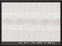
Now, researchers at the University of Würzburg (Würzburg, Germany) and Alcatel (Marcoussis, France), have realized an indium gallium arsenide phosphide (InGaAsP) PC laser based on a coupled-cavity waveguide (CCW), meeting these requirements.1 The two-dimensional PC lattice is formed by air-filled microholes in a 120° geometry with a lattice constant of approximately 350 nm; the crystal is air-filled to a 28% fill factor (see figure). In 40 adjacent hexagonal areas, the lattice holes are missing. The laser active layer contains four compressively strained InGaAsP quantum wells within a waveguiding layer (providing vertical light confinement) and is situated about 1.8 µm below the surface.
Tightly placed next to each other, the hexagons form an array of coupled-defect optical cavities. With and without electrical pumping, the coupled cavities allow radiation of selected wavelengths within the photonic bandgap to propagate along the array axis, thus making up the CCW. Those wavelengths are grouped in minibands. The number of modes in a miniband increases with the number of coupled cavities, with one cavity producing the typical Fabry-Perot modes and an infinite number of cavities producing a continuum. A photon of a wavelength within a miniband (generated in one cavity) propagates back and forth along the cavities so that its effective group velocity is slowed down, increasing its interaction time with the active medium.
Predictions show that the group velocity approaches zero for wavelengths approaching the band edge and that the gain increases to maximum there.2 In the case of coupled cavities, this should happen for waves with wavenumbers of 0 and p/R, where R is the distance between cavity centers.
Single-mode lasing
The authors generated single-mode lasing in their CCW at the long-wavelength band edge of a miniband in continuous-wave operation at 1530 nm. The long-wavelength edge has the best spectral match to the material gain. For even shorter wavelengths, a stop band that is part of the photonic bandgap shows strongly reduced intensity. At longer wavelengths, low-intensity oscillations occur that can be attributed to other allowed miniband modes defined by the 40 coupled resonators. Their intensity increases near the laser line, which is consistent with the slowdown of the group velocity near the band edge.
A 135-µm-long array produces single-mode radiation of 2.6 mW at room temperature with a threshold current of 15 mA. The optical-to-electrical efficiency is 4%. The laser emission is very stable and remains single-mode even at higher driving currents. By using different photonic-lattice constants and cavity sizes, lasing at different wavelengths within the material gain could be achieved—useful for wavelength-division multiplexing. Further, the principle can be applied with different gain media.
REFERENCES
- T. D. Happ et al., Appl. Phys. Lett 82(1) 4 (2003); ([email protected]).
- J. P. Dowling et al., J. Appl. Phys. 75(4) 1896 1994).
About the Author
Uwe Brinkmann
Contributing Editor, Germany
Uwe Brinkmann was Contributing Editor, Germany, for Laser Focus World.