Newsbreaks
Spectral shaper exploits micromirror array
A fiber-coupled spectral-shaping instrument commercially introduced by Newport (Irvine, CA) contains at its heart the digital micromirror array developed by Texas Instruments (TI; Dallas, TX), which is already used widely in projection displays. Although the TI device has become a research tool in many areas outside its originally intended use, the Newport application is one of the first commercial uses of the micromirror array other than in projectors. The instrument, a programmable spectral processor, is intended for precision optical applications in remote fiberoptic sensing, optical telecommunications, and life- and health-science markets.
The fiber-coupled instrument generates static or time-dependant spectral profiles over its 1520- to 1620-nm operating range with a resolution of 0.4 nm, applying an arbitrary transformation to the original optical signal bypassing selected narrow-wavelength bands and blocking others. The technology is based on Cidra's (Montreal, Quebec, Canada) use of the TI micromirror array, in which a diffracted spectral profile is transformed into an optical output. Because the Newport device can programmably simulate optical filters, it can also be used in optical-filter design and wavelength-division-multiplexing simulation. Contact Ron Hartmayer at [email protected].
Air-gap filter tunes over a 127-nm range
An electrostatically tunable air-gap filter fabricated by researchers at the University of Kassel (Kassel, Germany) and the Royal Institute of Technology (Kista, Sweden) provides a tuning range of 127 nm at a 7.3-V voltage for light in the 1550-nm range. The filter, which has a multiple (2.5-period) air gap and is made of indium phosphide (InP), could become the key component of tunable receivers for wavelength-division multiplexing.
Three 3l/4 indium phosphide (InP) membranes either 20 or 40 µm in diameter are spaced by l/4 air gaps and are supported by three or four thin, flexible suspension beams. Because the index-of-refraction difference between air and InP is large, the filter is tolerant of variations in air-gap thickness. The filter performance was characterized with direct single-mode fiber coupling and an erbium-doped fiber amplifier as a broadband source. The dip in reflectance had a full width at half maximum (FWHM) of 3 nm for devices with 20-µm-long suspension beams and 7 nm for those with 40-µm-long beams. Since calculations showed 1-nm FWHM for flat membranes, membrane bending was considered to be the cause of the broadening. Contact Hartmut Hillmer at [email protected].
Joined diamond and aluminum nitride emit light
Combining diamond and aluminum nitride (AlN)—two wide-bandgap semiconductors—into one device may one day lead to short-wavelength ultraviolet light-emitting diodes and lasers. Joining the two dissimilar materials (AlN has a wurtzite structure, while diamond is cubic) together is not easy, however. Using plasma-induced molecular-beam epitaxy, researchers at the Technische Universität München (Garching, Germany) are doing just that. A silicon-doped AlN film on a naturally boron-doped diamond substrate forms a heterobipolar diode that emits light in the 2.7 to 4.8-eV (442 to 250-nm) region.
To make the device into a light emitter, the researchers evaporated titanium aluminum ohmic contacts onto both sides of the sample. The 2 × 2-mm device showed pronounced rectifying properties, with a relatively high leakage current in the reverse direction ascribed to structural defects at the AlN/diamond interface. Room-temperature electroluminescence measurements were taken with a double-grating monochromator and a photomultiplier tube. The sample emitted bright blue light peaking at 2.7 eV and a secondary peak at 4.8 eV that was 1% as bright as the blue emission, both peaks showing only under forward bias. Contact José Garrido at [email protected].
Electrically pumped cadmium sulphide nanowires lase
Scientists at Harvard University (Cambridge, MA) have made individual cadmium sulphide nanowires into electrically pumped lasers. The nanowires must have a diameter of at least 70 nm to support a single transverse mode at a 510-nm wavelength. After placement on a heavily doped silicon-on-insulator substrate, a nanowire is held in its spot by overcoated aluminum oxide, titanium, and gold. One end of the wire is left uncovered. When driven at room temperature by an injection current of 210 µA, a representative nanowire emits many Fabry-Perot modes with a spacing of 1.83 nm. When the laser is cooled to 8 K, it emits a single peak at 494 nm.
The multimode room-temperature spectrum of this emitter is characteristic of a laser driven just above threshold. Injection nonuniformity resulting from nonideal material interfaces limits the laser as fabricated to being operated at just above threshold. Bragg gratings instead of cleaved ends, and core/shell nanowire structures, should improve operation. Electrically pumped nanowire lasers of gallium nitride and indium phosphide are possible, say the researchers. Contact Charles Lieber at [email protected].
Volume hologram is fabricated layer by layer
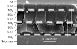
Volume holograms are usually created by exposing a photosensitive medium to interfering light. In a different approach, researchers at the University of Alabama in Huntsville (Huntsville, AL) are building volume holograms a bit at a time by stacking binary gratings that have offsets to emulate Bragg planes. An example hologram contains three high-refractive-index titanium dioxide gratings separated by layers of SU-8 (a low-index polymer material), with the bottom grating resting on a glass substrate. The most-challenging fabrication step is the offsets between the grating layers.
To achieve the proper offsets, a high-precision layer alignment technique for a contact mask aligner was developed based on double diffraction between the previously fabricated grating on the substrate and the grating on the photolithographic mask. Offsets were easily controlled to within the 100-nm tolerance (layer thicknesses, however, were not optimally controlled). The volume hologram was tested with 2.05-µm light to determine its angular sensitivity. The measured peak diffraction efficiency exceeded 80%, but is sensitive to Fresnel reflections between grating layers. A hologram of this type will be used as a beam-deflection and scanning element in a coherent lidar system. Contact Diana Chambers at [email protected].
Light-emitting diodes on silicon exploit nanoparticles
Although the indirect bandgap of silicon (Si) prevents it from being fabricated into light-emitting diodes (LEDs) in the ordinary way, research groups around the world are trying to work around this problem, with the goal being Si LEDs and other optoelectronics mass-producible like today's integrated circuits. At Photonics West 2003 (Jan. 25–31; San Jose, CA), scientists from National Taiwan University outlined two of their approaches (neither of which as of yet produces efficient emitters).
In one scheme, a layer of 8- to 12-nm-diameter silicon dioxide nanoparticles is deposited on Si between a back electrical contact of aluminum and a front contact of silver paint. Upon application of an electric field, the silver migrates into the nanoparticle layer. Although efficiency is only 1.5 × 10⁻⁴, near-lasing action has been seen from the 1-mm-diameter device, with its spectrum showing resonance peaks. In the other technique, suspended cadmium sulfide particles 5 nm in size are spun onto a silicon substrate (room-temperature evacuation fixes the particles in place). Emission is at 571 nm, with a spectral full-width at half-maximum of 29 nm. Efficiency is approximately 10-5. Contact Ching-Fuh Lin at [email protected].


