Silicon yields light two ways
Investors may have taken some of the money out of optoelectronics, but the fact that two different research teams on two different continents are rapidly closing in on silicon light-emitters using two different methods indicates once again that the innovators are still playing for keeps.
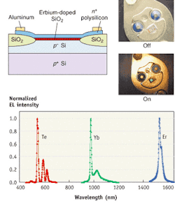
At the annual SPIE Photonics West conference in January, U.S. researchers led by Bahram Jalali at the University of California-Los Angeles (UCLA) gave an update on their observation of a Raman effect in silicon waveguides, which presents a potential alternative to the rare-earth-doped silicon light-emitters announced by ST Microelectronics (Geneva, Switzerland) last fall (see figure).
As with the erbium doping of silicon following upon the successful erbium doping of optical fibers for telecom applications, the UCLA Raman approach basically involves scaling down the Raman fiber-amplification processes used in optical communications.
"In fiber you typically need several kilometers for Raman amplification because the interaction is very weak," Jalali said. "Obviously when you talk about silicon chips, the dimensions are at most millimeters. So you are off by several orders of magnitude."
Jalali's research group realized, however, that the crystalline structure of silicon concentrates the Raman gain interaction about four orders of magnitude more strongly than does the amorphous structure of optical fiber. Another two orders of magnitude of light-intensity increase was gained by the factor of 100 decrease in cross-sectional area in going from an optical fiber to a silicon waveguide.1
"We gain a factor of 100 here and a factor of roughly 10,000 from the strength of the interaction because of the single-crystal vs. amorphous difference," Jalali said. "So the one million times stronger effect in a silicon waveguide than we have in the fiber allows us to achieve Raman light generation in millimeters of waveguide."
A first step
A potentially attractive feature of the UCLA approach is that the effect was observed in conventional waveguides that had not even been optimized to produce the effect. Therefore, once the procedure moves from its current R&D stage into a production environment (assuming that the current level of simplicity is maintained), it is likely to prove readily adaptable to existing silicon fabrication facilities. Jalali emphasized that observing spontaneous Raman emission from silicon waveguides is only a first step.
"The next step is to demonstrate and observe stimulated emission, which is needed for amplification and lasing," Jalali said. "That is a step we're working on right now. But based on the value for the Raman efficiency that we measured from the spontaneous emission, we are confident that efficient amplification and lasing should be possible in silicon waveguides."
He expects to achieve stimulated emission within the next year, but the production of a useful device will probably entail solving what Jalali described as the engineering problem of optimizing silicon waveguides to produce sufficient gain.
Jalali added that another potential advantage of their method might lie in the fact that emission wavelengths for doped materials depend upon the dopant, while Raman emission is a function of pump wavelength. Of course, a strong advantage of the rare-earth-doped technology is that ST Microelectronics is already producing devices.
The ST technology was developed in Catania, Sicily, at the Corporate Technology R&D Organization using the same pilot line that ST uses to develop new metal-oxide semiconductor field-effect-transistor and bipolar devices, which has allowed the company to accelerate the transfer from proof-of-concept experiments to prototype development and industrialization.
"The quantum efficiencies achieved [using rare-earth-doped silicon] are about 100 times better than has previously been possible with silicon and are, for the first time, comparable to those obtained from GaAs and other compound semiconductors traditionally used to make light-emitting diodes," said Salvo Coffa, manager of the research team at ST.
Jalali also expects to achieve such efficiencies. "I think we can look forward to a new era for optical devices in which we make use of good old silicon to make the devices instead of having to rely on more exotic material and devices," he said. "That doesn't mean that silicon is going to completely replace gallium arsenide and indium phosphide for this purpose, but I think there could very well be commercial silicon optical devices on the market that perform a subset of the functions performed by the indium phosphide, gallium arsenide devices."
REFERENCE
- R. Claps et al., Optics Express 10(22) 1305 (Nov. 4, 2002)

