Inductive storage yields efficient power alternative
Traditional laser-diode power supplies are designed using a linear regulator, a switch-mode regulator, or a pulse-forming network, but these designs encounter serious limitations at high current levels due to excessive power dissipation and current sense/control-loop limitations. A power supply based on inductive rather than capacitive energy storage and incorporating a hysteretic, current-mode, buck regulator can address these concerns at a competitive cost.
Conventional design limitations
Linear power-supply designs suffer from large energy storage requirements—requiring large capacitor banks—and significant power dissipation. With a typical efficiency of 50% or less, the problem is magnified at higher currents, thereby limiting the maximum duty cycle of the device.
Switch-mode regulators are more efficient, but have bandwidth limitations that are difficult to overcome. In pulsed operation, the sampling frequency typically must be at least 10 times the output frequency, which implies that a driver capable of operating at 100 kHz must have a regulator switching frequency of at least 1 MHz. Such switching frequencies present a number of design challenges for the design engineer.
Designs based on a pulse-forming network (PFN) are limited to fixed rather than variable pulse widths, with very limited maximum pulse widths and limited pulse repetition frequency. Although PFN designs are an excellent choice for very narrow pulse width, high-current drivers such as those used in rangefinder and LIDAR applications, they are not well suited to longer pulse width and quasi-CW (QCW) applications.
The current regulator for high-current supplies must be efficient, and for many laser-diode applications must be suitable for pulsed and QCW operation. Both linear and switch-mode designs require a feedback loop to control the output current. Some of the limitations experienced by both linear and switch-mode regulators are in the very nature of closing feedback loops with sufficient bandwidth to produce pulse waveforms with submicrosecond rise and fall times. A key component of the feedback loop is the current sensor. The current sensor must offer the bandwidth necessary to track the output-current waveform. To keep dissipation minimized, a low value resistor in the current path is often utilized as the current sensor.
Low-value resistors used as current sensors are, as with all components, plagued with stray elements. In this case inductance is a major stray element and directly affects the accuracy of the current sensor. A sense resistor with too high inductance will give edges with overshoot and rise times that actually are not present in the current pulse.
The accuracy problem is tied to a very simple concept of an L/R time constant. The current decay in an LR circuit is related to time by
I = Ioe(-t/τ)
where τ is the L/R time constant and Io is the initial current. For the current rise time, the formula is:
I = Io[1-e(-t/τ)]
Practical resistance values for currents in the 100-A or greater range become limited by power dissipation. A simple 0.001 Ω resistor at 100 A produces a low-amplitude signal of 0.1 V and dissipates
P = I2R or 1002*0.001 = 10 W.
If the time for the current to settle due to the inductance of the resistor is approximately three time constants (3τ), then for a given rise time there is a maximum inductance the resistor can have. As an example, if the edges are 1 µs, then the time constant τ = 1/3 or 0.33 µs. This implies that the maximum inductance of the resistor is L = R*0.33E-6 = 0.001*0.33E-6 or 333 pH. A resistor with inductance this low is not readily available. Practical available parts are in excess of several nH. Therefore, current measurement with very low resistance values is not easily achieved with high current and fast edges.
Beyond traditional limits
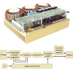
To overcome the limitations of linear and switch-mode regulators, and the severe limitations of the current sensor at high currents, we developed a driver using inductive energy storage with a hysteretic, current mode, buck regulator (see Fig. 1). Here, the DC current in an inductor is measured and controlled by the high-efficiency, current-controlled, hysteretic regulator rather than the actual modulated output current.
null
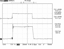
This regulator controls the current between an upper bound and a lower bound. Its pulse width and switching frequencies are both agile. The regulator is "on" until it reaches the upper bound and is "off" until it reaches the lower bound. This results in a very responsive regulator with one penalty, current ripple. The current ripple is the ripple necessary from having an upper and lower current boundary (see Fig. 2). In most laser-diode applications, 1% to 2% ripple is not a problem. By accepting this higher ripple, a current sensor with a much slower response time can be used to control the current in the inductor rather than a high-speed current sensor to measure the actual output. In this design, we used a hall-effect closed-loop sensor.
null
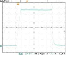
To operate the driver in a pulsed or QCW mode, a crowbar switch is used across the output of the current regulator to short out the current source. When a pulse is desired, the crowbar switch is opened and the current source is then able to drive the laser. When the switch closes the current is diverted away from the laser. Current stored in the inductor appears as a current source and therefore has a large compliance range with a leading edge defined by circuit capacitance in the crowbar switch and other strays. The inductive driver operates on 24 V DC, providing a maximum voltage compliance of about 22 V. The wide compliance range therefore allows the supply to power diodes with forward voltages from <2 to 22 V with no adjustments or tuning of the driver or supply voltage (see Fig. 3).
null
The crowbar circuit is important in reducing power dissipation and controlling the leading and trailing edges of the laser driver. This requires a very low "on" resistance and low capacitance. The edges are not identical in the way they are controlled. The falling edge is controlled by the inductance in the circuitry after the crowbar switch, and the speed of the crowbar switch itself. The crowbar switch shorts out the current source as well as the external circuit connecting the laser diode to the driver. This would seem to be a way of obtaining a very fast turn-off of the laser diode but the external circuit inductance will actually be the controlling factor.
The circuit that includes the laser diode is made up of the laser diode, stray inductance, and the resistance of the crowbar. The resistance of the crowbar is very low, so the laser is the only place to dissipate any stored energy from the stray inductance. This time is related by V = L(di/dt) where the V is the laser forward drop, L is the stray inductance, di is the amount of current change and dt is the time required. For a typical diode the forward drop is 2 V, the current can be 100 A and the stray inductance 50 nH. The time for the current to decay is dt = L(di)/V = 50 nH*100/2 = 2.5 µs. This fall time may be too long for some applications. Therefore care must be exercised to reduce stray inductance.
CHARLES COLEMAN is a senior design engineer and RON SHERWOOD is president of Directed Energy, 2401 Research Blvd, Suite 108, Fort Collins, CO 80526; e-mail: [email protected], [email protected].


