Newsbreaks
Diffractive lenses on VCSELs are suited for wafer-scale fabrication
As a result of their geometry, vertical-cavity surface-emitting lasers (VCSELs) have enabled wafer-scale fabrication of semiconductor lasers. Now, researchers at Heptagon and the Centre Suisse d'Electronique et de Microtechnique SA (both of Zurich, Switzerland) have carried the wafer-level process a step further, creating a technique to add diffractive optical microlenses to VCSELs via wafer-scale fabrication; the lenses serve to couple the laser light into an optical fiber.
The lens material is an organically modified ceramic that, when ultraviolet (UV) cured, becomes a thermally stable glasslike amorphous composite. A 200- to 400-µm-thick layer of the material mixed with a photoinitiator is deposited on the VCSEL-containing wafer; a robot-positioned UV-transparent replication stamp forms the lens or lens array, which is cured and then thermally annealed. The researchers fabricated single fourth-order diffractive lenses; the elements achieved coupling losses of less than 0.5 dB into a 50-µm-core optical fiber for lateral alignment tolerances of ±10 µm, sufficient for passive fiber alignment. In large-scale fabrication, masks would block UV from areas between the lenses, allowing selective curing; uncured portions of material between the lenses would then be washed away. Contact Thomas Ammer at [email protected].
Fiber sensor measures curvature
One common use of optical-fiber sensors is in measuring the deflection of mechanical structures by sensing strain. Strain sensors have their limitations, however; for example, very thin beams deflect appreciably even with little strain. In addition, a fiber sensor's very presence in a structure can alter the strain in its vicinity, causing measurement errors. Researchers at the City University of Hong Kong (Kowloon, Hong Kong) have developed a fiber sensor that measures another result of deflection—a change in the radius of curvature. Curvature remains significant for the deflection of thin beams; it also is not changed by the presence of the sensor.
Fabricating the sensor involves cutting to the core of the fiber (for example, a 0.25-mm-diameter plastic fiber) over a length equal to a few diameters, leaving a rough surface. A portion of the light propagating through the fiber is scattered out of the fiber at the rough surface; the transmission drop depends on the fiber's curvature. In one example, the sensor measured a 510-mm-long beam to a deflection resolution of 0.072 mm, or a radius of curvature of 1.54 km. Contact Alexandar Djordjevich at [email protected].
OLED color can be chosen after fabrication
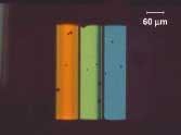
An organic light-emitting device (OLED) with a color that is configurable after fabrication has been developed by researchers at National Taiwan University (Taipei, Taiwan). The device contains three layers of different organic light emitters separated by two layers of molecular glasses that have differing above-room-temperature glass-transition temperatures.
In the as-fabricated state, the OLED emits blue light. To change the device to a green emitter, it is heated above 95°C, causing the first molecular glass to soften, mixing the blue- and green-emitting layers and allowing holes to get to the green layer. To alter the device so that it emits red, it is heated above 125°C causing the second molecular glass to soften, mixing all three layers. An OLED with three adjacent 12 × 80-µm emitters—red, green, and blue—was fabricated by thermal annealing caused by heating of transparent indium tin oxide electrodes; their brightnesses were 10,000, 40,000, and 30,000 cd/m2, respectively. Such a device could be patterned into a full-color OLED display using thermal-imaging techniques rather than heated electrodes, say the researchers. Contact Chung-Chih Wu at [email protected].
Single-mode ring laser diode emits stably and unidirectionally
Ring-waveguide semiconductor lasers eliminate potential spatial hole-burning effects of ordinary linear-waveguide semiconductor lasers and may thus become useful in telecommunications. But stable single-mode unidirectional operation of a ring laser diode is hard to achieve. Now, scientists at Julius-Maximilians-Universität Würzburg (Würzburg, Germany) have done just that, fabricating a 600-µm-long oval-racetrack-shaped ring waveguide laser together with an inner S-shaped waveguide connecting to the oval and a lateral metal distributed-feedback grating deposited on both sides of the straight sections of the "racetrack." For experiment, two output waveguides extract both clockwise (CW) and counterclockwise (CCW) modes.
The waveguides are fabricated by electron-beam lithography and dry etching; the grating is patterned by electron-beam lithography. With no grating, mode competition between oppositely circulating modes causes fluctuations in the desired mode. Introducing the grating eliminates mode jumps and changes in mode order. The S-shaped waveguide section enhances light output in the CW direction. The CW output of 17 mW/A is 4.6 times higher than the undesired CCW output. The output is at a 1003-nm wavelength and exhibits a 37-dB side-mode-suppression ratio. Contact Sven Mahnkopf at [email protected].
Curved filter corrects color of metal-halide-lamp fiber sources
Optical fibers into which white light is coupled can serve as illuminators for critical applications such as surgery. The standard white-light source, the xenon short-arc lamp, produces very high-quality white light with a color-rendering index (CRI) of 98 or better (a CRI of 100 is perfect; 90 is good enough for critical applications). The xenon lamp has a low luminous efficiency of 20 lumens/W, however, as well as a lifetime of less than 1000 hours. One alternative—the metal halide lamp—is very efficient (55 to 75 lumens/W) and lasts at least 2000 hours, but has a CRI of only 60 to 70 as a result of three sharp spectral lines.
Engineers at the Rockwell Collins Advanced Technology Center (Cedar Rapids, IA), Cogent Light Technologies (Santa Clarita, CA), Rockwell Scientific (Thousand Oaks, CA), ZC&R Coatings (Torrance, CA), and Ushio America (Irvine, CA) have developed a dual-notch thin-film dielectric filter that brings the CRI of a metal-halide lamp up to above 90 by reducing the strength of the spectral lines while leaving the continuum alone (one of the notches encompasses two of the three lines); the filter is on a spherical substrate optimized for a converging light beam for fiber-coupling. Contact Ronald Ferrante at [email protected].
Backside irradiation and microspheres create nanoscale arrays
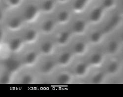
Periodic nanoscale surface patterns on glass surfaces can be used as polarizing beamsplitters and other optical components. Patterning techniques can take the form of photolithography or ablation through a near-field optical probe; another technique relies on depositing a monolayer of nanospheres, which is then irradiated to produce arrays of depressions as a result of intensity enhancement from scattering and the near-field effect. Researchers at the University of Texas (Austin, TX) have developed a variant of the nanosphere technique that minimizes scattering, producing nanoscale patterns based on near-field intensity enhancement alone. The resulting intensity enhancement between the spheres and the glass surface approaches a factor of 100, producing nonlinear absorption that creates the pattern.
Silica spheres 640 nm in diameter were arrayed hexagonally on the surface of a borosilicate glass substrate. The spheres were irradiated with 10-ns pulses from a 1064-nm-emitting Nd:YAG laser at a fluence of 3 J/cm2; irradiating from the backside of the substrate eliminated scattering. The spheres were then washed away. The resulting depressions were 350 nm in diameter and spaced 640 nm apart. Contact Shaochen Chen at [email protected].
Polarization helps reduce focal-spot size
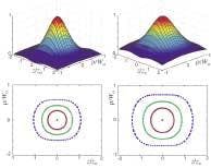
Pushing the size of a focal spot below the conventional diffraction limit can benefit microscopy, photolithography, and other optical applications. Apertures that modify phase and amplitude can reduce the volume of the focal spot, as can nonlinear processes such as two-photon absorption. Now, researchers at Boston University (Boston, MA) have developed a polarization-assisted superresolution technique based on two orthogonally polarized Gaussian beams with a relative 90° phase shift and an offset of half the Rayleigh range. The combination produces two independently propagating non-Gaussian beams, one of which has a smaller focal volume than the original Gaussian beam (superresolved beam profile is on left; Gaussian beam profile is on right).
The researchers attribute the smaller focus to the interference of two wavefronts with different curvatures, producing an annular distribution of the beam. Even if produced in other ways, such a non-Gaussian wavefront would focus to the smaller volume, say the researchers. In an experiment, the focus of a beam of 1-µm laser light was reduced in size by a factor of at least 1.4 over the input beam, with the tighter beam carrying 11% of the input power. Contact Bahaa Saleh at [email protected].
Decision nears on camera type for LSST
A large ground-based telescope is being designed that, if built, would search the cosmos for dark matter and energy by measuring weak gravitational lensing caused by distant galaxies and other objects. The telescope, which in one configuration would have a diameter of 8.4 m and an effective aperture of 6.9 m, is called the Large Synoptic Survey Telescope (LSST) and is being collaboratively designed by groups in industry and academia. One important decision yet to be made is on the camera itself—should it be CMOS (complementary metal-oxide semiconductor), or CCD (charge-coupled device)?
The 2.3-gigapixel camera would be made of 2k × 2k (or larger) modules butted together; quantum efficiency (QE) needs to be 90% over a 400- to 1000-nm spectral range. "In 1980, CCDs were the only choice," notes project director Anthony Tyson of Lucent Technologies Bell Labs (Murray Hill, NJ). "But Moore's Law is powerful. Now [with CMOS] you can have many transistors under each pixel. Hybrid p-i-n diode CMOS arrays have high QE and low noise, more than competitive with CCDs. Prices on hybrid p-i-n diode arrays are high now, but in quantity that should come down." Contact Anthony Tyson at [email protected].
Safer gas replaces phosphine for semiconductor laser manufacture
Phosphine gas (PH3) is the source of phosphor in the fabrication of aluminum gallium indium phosphide (AlGaInP) semiconductor lasers—the ubiquitous red-emitting lasers found in compact-disk players, barcode readers, and printers. Phosphine is also highly toxic, causing pulmonary edema and interfering with metabolic enzymes. Researchers at Nanyang University and the Institute of Materials Research and Engineering (both of Singapore) have come up with an alternative AlGaInP phosphor source: the much-safer tertiarybutylphosphine (TBP).
Using metalorganic chemical-vapor deposition, the researchers grew AlGaInP epilayers and AlGaInP/GaInP multiple-quantum-well (MQW) structures with TBP, then obtained their photoluminescence spectra. The results indicated optical quality as good as structures grown with PH3. Next, they fabricated crude electrically pumped AlGaInP MQW lasers using TBP. The lasers, which had no lateral carrier confinement, no efficient heat sink, and no facet coatings, emitted at 647 nm under pulsed conditions only, but illustrated the utility of TBP. To further confirm the use of TBP as a phosphor source for semiconductor-laser manufacture, the researchers are currently fabricating higher-quality lasers to achieve continuous-wave operation. Contact Jian-Rong Dong at [email protected].


