Gallium arsenide emits at telecom wavelengths
Researchers at Yale University (New Haven, CT) have taken an important step toward monolithically integrating longwave light-emitting components into a commercially established semiconductor substrate material for integrated optoelectronics by successfully demonstrating the first 1.5-µm-emitting gallium arsenide (GaAs) light-emitting diode (LED).
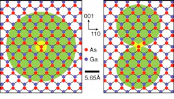
Instead of relying on the natural 0.85-µm bandgap energy of GaAs, the Yale team used molecular beam epitaxy (MBE) of low-temperature -grown GaAs to create artificial deep energy-level bands; located between the usual conduction and valence bands, they rely on arsenic antisite defects in which gallium atoms are displaced by arsenic atoms. The arsenic antisite defects emit light during transitions from the ground states, for which the schematic shows two constituent cloud shapes of an antisite in a GaAs lattice (blue is gallium and red is arsenic; green and yellow are electron clouds). The researchers observed strong optical-emission peaks at 1 and 1.5 µm.1
The large density of arsenic antisite defects yielded large absorption coefficients and efficiency-bandwidth products for deep-level optical transitions, on the order of conventional conduction-to-valence band transitions. In addition, subpicosecond carrier lifetimes in the low-temperature-grown GaAs are expec ed to enable rapid switching. The research team reported 24 mW of internal optical power and projected modulation at terahertz rates.
"This result is important for three reasons," said Janet Pan, a professor of the departments of electrical engineering and applied physics at Yale. "First, 1.5 µm is the preferred wavelength for efficient transmission (least loss) over long distances in glass optical fibers. Second, GaAs is the most established technology for inexpensive reliable integrated optoelectronics. And third, our light emitters can be turned on and off at terahertz speeds, which are needed for future high-speed communications systems."
The indium phosphide substrate upon which 1.5-µm-wavelength optical devices are usually made has not proven compatible with commercial integrated circuit technology, so the Yale results seem to offer a lot of promise for integrating fiberoptic components with electronic circuitry. But Pan expects that it will take three to five years before practical devices result from the long-wavelength GaAs LED technology. The next goals for the research team will be to increase the efficiency above the reported 0.6% and to decrease operating-current levels.
"I would describe my approach with caution," Pan said. "As with any new material and any new technology, unforeseen problems come up and have to be solved. The internal optical power within my LED was large. However, much engineering will be required to extract the internal optical power as external optical power."
REFERENCE
- J. L. Pan et al., Nature Materials, published online, www.nature.com/naturematerials.com, doi:10.1038/nmat887 (May 4, 2003).

