Nontraditional material systems may yield cheaper solar cells
In a traditional silicon (Si)-based solid-state photovoltaic cell—built largely upon experience gained in the semiconductor industry—very pure and hence very expensive Si is required to convert sunlight into electrons and holes, while simultaneously generating an electric field by conducting the charge carriers to current collectors. Potentially less expensive and more easily manufactured solar-cell material systems described at the San Francisco, CA, meeting of the Materials Research Society in April, included a Shottky diode design from the University of California Santa Barbara (UCSB) in which the photoabsorption step is physically separated from charge collection.
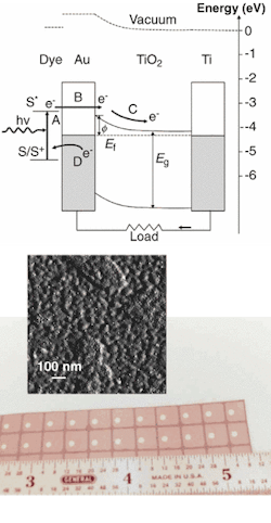
Photon absorption in the multilayer UCSB device occurs in a photoreceptive layer, consisting of semiconductor quantum dots in one instance and of a photosensitive dye in another, adsorbed onto the surface of a thin gold film (see figure). The opposing surface of the gold film contacts a thin layer of titanium dioxide, such that spontaneous electron flow from the titanium dioxide semiconductor to the metallic gold creats a local electrostatic field (or Shottky barrier to electron flow) by leaving a slight negative charge on the gold and a slight positive charge on the titanium dioxide.
Light falling on the photoabsorption layer of the device releases electrons into the conduction band of the gold layer with enough energy to penetrate the Shottky barrier and enter the titanium dioxide semiconductor conduction band. The semiconductor then transports the electrons to a current collector in the form of a titanium support, which conducts the electrons to an external circuit. The UCSB researchers reported an internal quantum efficiency of electrons measured per photon absorbed on the order of 10%.1
Cadmium selenide/cadmium sulfide nanoclusters on a gold film form the active region of a solar cell. To make large-enough Shottky barriers for the solar cell, researchers at UCSB had to develop commercially adaptable laboratory methodologies for inexpensive electrochemical deposition over large areas of electrically continuous, 10-Å-thick metal films. In actual devices, light falling on the photoreceptor releases electrons that cross a Shottky barrier en route to an external circuit (top). Quantum-dot photoreceptors promise better stability and flexibility than photosensitive dyes (bottom).
"We've simply shown that this other route to transforming photons into useful electrons does work; whether or not it works efficiently in a practical system remains to be shown," said Eric McFarland, who directs the UCSB research team. "Our devices aren't nearly efficient enough for any kind of commercial application. It's the potential for an inexpensive device that we've shown. We've used the fact that electrons can travel reasonably long distances in very thin noble-metal films without losing their energy."
Excited electrons can travel as far as 20 to 50 nm in noble metals, and the gold film in the UCSB device is only 10 nm wide. Another possible explanation for the observed phenomenon is that electrons in the gold film are excited by energy transfer from the dye layer and then injected into the titanium dioxide conduction band.2
"People who have been working on artificial photosynthesis have used electron transfer from excited dyes through gold particles for chemical reactions as well," McFarland said. "They have captured the electron energy in a gold particle and used the energetic electron to do chemistry.." In fact, the UCSB team had originally investigated the method of thin-film-diode charge collection for studies of fundamental interactions of gas-phase reactants on metal surfaces, particularly for using ultrathin metal fills on diodes to monitor ballistic electrons that were produced from chemical reactions on surfaces.3
"Following along that same line, we thought we might be able to produce excited electrons, not just from chemical reactions, but also from photon excitation of molecules on the surface of a metal film and then capture those energetic electrons in the same way that we are capturing energetic electrons in our sensors," McFarland said. "The real benefit would be that these could be manufactured very cheaply. In the end, they won't be more efficient than an ideal p-n junction semiconductor solar cell. But they could be almost as efficient and they could be a lot cheaper."
In a traditional silicon (Si)-based solid-state photovoltaic cell¿built largely upon experienc
Because the device is based on majority carriers (electrons) only, it should prove less sensitive to impurities and imperfections than Si-based semiconductor solar cells. At the Spring MRS meeting, UCSB researchers reported open-circuit voltages of 0.34 V and short-circuit current densities of 0.12 mA/cm2 under simulated broadband illumination of 100 mW/cm2, when the dye merbromin was used as a photoreceptor. Short-circuit current density fell to 0.05 mA/cm2 when the dye was replaced with 5-nm cadmium selenide/cadmium sulfide semiconductor quantum dots under the same illumination.
Because of potential problems with dyes such as photo-oxidation, McFarland expressed a preference for the tunable and more-stable semiconductor quantum dots, while adding that numerous other photon-capture structures are also available and under investigation. The ultimate viability of this approach, however, will depend upon improving the internal quantum efficiency (IQE). "If a photon is actually absorbed in the photon-capture structure, the IQE is the probability of that electron getting from the dye and into the semiconductor where it can be used in a circuit; right now, the device IQE is approximately 10% and needs to be upwards of 90% before it's going to be viable," he said.
To solve that problem, McFarland's team hopes to improve the electronic coupling between the photoabsorber and the noble metal without adversely affecting the photoabsorption properties. "There is a tradeoff between being able to absorb well and being able to transfer the electron well," he said. "So we are working on that with different kinds of molecules that will give us covalent coupling between the metal film and the photoreceptor. But that may take a lot of work and a long time."
REFERENCES
- E. W. McFarland, J. Tang, Nature 421, 616 (Feb. 6, 2003).
- M. Grätzel, Nature 421, 586 (Feb. 6, 2003).
- B. Gergen et al., Science 294, 2521 (Dec. 21, 2001).

