Quantum dots pave way for polymer-based optical chips
Researchers at the University of Toronto (Toronto, Ontario, Canada) have developed a hybrid plastic embedded with quantum dots that can produce coherent light in the 1.3- to 1.6-µm range.1 They believe that their work could help lead to the integration of several fiberoptic communications devices on a single chip.
"We have shown that our hybrid plastic can convert electrical current into light with promising efficiency and with a defined path toward further improvement," said Ted Sargent, professor of electrical and computer engineering. "With this light sourced combined with fast electronic transistors, light modulators, light guides, and detectors, the optical chip is in view."
According to Sargent and his colleagues, polymer-quantum-dot nanocomposites have been investigated for visible-spectral-region luminescence and photovoltaic properties. By extending them into the infrared, they could potentially enable planar-integrable active optical elements suitable for telecommunications applications in the 1.3- to 1.6-µm range (see figure).
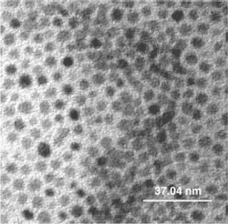
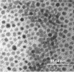
To demonstrate this, the research team created nanocrystals of lead sulfide (PbS) using a technique that allowed them to work at room pressure and temperatures below 150°C. They chose PbS because it has a larger band-gap than other lead-based materials and thus does not require ultrasmall nanocrystals to adjust the effective gap in the spectral region suitable for telecommunications applications.
The nanocrystals were synthesized in solution, and lead oxide was dissolved in oleic acid at 150°C, to which the sulfur precursor was added. The resulting PbS nanocrystals were kept apart from one another using a capping layer of oleate ligands (organic molecules) coordinated to the lead atoms. The particle size was tunable by varying the conditions of growth. They replaced the oleate ligands with shorter chains to reduce the thickness of the electrically insulating capping layer surrounding the nanocrystals and increase their stability.
The crystals were then combined with a semiconducting polymer material to create a thin, smooth film of the hybrid polymer. The precipitated nanocrystals were redissolved in the organic solvent needed for fabricating the polymer composite. A polymer precursor was combined with the solution of nanocrystals in toluene. The solution was coated onto a glass substrate covered by a transparent anode contact. Following the100- to 150-nm-thick nanocomposite layers, an upper cathode contact was fabricated by vacuum evaporation of magnesium and a thin-film cap of silver.
Controlled synthesis
According to Sargent, one major conclusion of the study was that choosing the length of the replacement ligands allowed the researchers to determine whether energy was transferred from the polymer to the quantum dots. Using their hybrid material, the researchers were able to generate a spectrum of light from 1.3 to 1.6 µm. Through controlled synthesis, they can maintain the average nanocrystal diameter to within a single layer of atoms, which enables them to control average spectral properties (peak wavelength) to within about 50 nm.
"This is nanoengineering," Sargent said. "We are customizing the molecules to wrap them around our quantum dots, and the molecules have to do two things: keep the dots separate from one another, and allow electrical energy to get into the dots so it can be converted into light."
There is still much more work to be done before this material will become practical enough for use in the telecommunications world, however. Sargent and his colleagues are already addressing such challenges as increasing the efficiency of converting electrons into photons and decreasing the voltage needed to pass significant current through the device. Once these challenges are overcome, they will need to begin integrating these materials with passive optical, electronic, and microwave circuitry and then investigate the reliability of the devices over long-term operation.
"What else needs to happen to make this practical is that these things need to be shown to work over several thousand hours, but there are a number of things that come even before that," Sargent said. "Before long-term operation, we need to understand the origins of why they are not as efficient as we would like them to be, and we need to make them more efficient."
REFERENCE
- L. Bakueva et al., Appl. Phys. Lett., 2895 (April 28, 2003).

