Seminar digs deep into manufacturing issues
Picking up where last year's conference left off, the second annual Strategies in Optoelectronics Manufacturing Seminar (April 15–16; San Mateo, CA) took a more focused look at automation, outsourcing, cost, yield, and other issues related to the fabrication of optoelectronic components. Reflecting how quickly this field is evolving, the talks were more pointed and dug deeper into these issues, prompting several friendly debates and much audience participation. In response to the industry's struggle to find new markets for what were originally intended to be optical-networking components, several talks also covered emerging opportunities in nontelecommunications fields, including biophotonics, nanophotonics, solid-state lighting, and smart sensors. Other sessions provided updates on roadmapping and standards efforts.
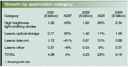
Tom Hausken began the event with a relatively positive presentation on the prospects for optoelectronic component sales, including a projection of 30% growth this year in the telecom market (see table). According to Hausken, with inventories finally being worked through, suppliers are beginning to ship more products. While 30% growth sounds like a lot, it still pales in comparison to industry revenues of three years ago.
"What is 30% in 2003 was hardly anything back in 2000. In fact, it could grow 50% or even 100% and people might hardly notice, since we have fallen so far down," Hausken said. "How could they not notice? Because there will still be companies going out of business. Even 100% growth would not be enough to save many companies."
In line with this, another underlying theme of the two-day event was cost reduction and yield improvement. Presentations on wafer-level integration, microelectromechanical-systems packaging, chip performance, fiberless mounting, and surface-mount procedures all included price performance as a key reason to consider these processes. In his talk on chip performance and package cost, for example, Alex Rosiewicz of EM4 Photonics (Burlington, MA) noted that while packaging contributes 50% to 80% of overall component cost, inconsistent chip performance also plays a major role.
"While package design can compensate for chip problems, it has a cost impact," he said. "It increases package complexity, materials cost, and labor costs and reduces yield. In the silicon industry, chips are very consistent, which leads to more-automated processes. Not so in the optoelectronics industry."
Process as product
Automation was another hot topic at the seminar, and the panel session "The Question of Automation" sparked several extended discussions both during the panel and throughout the rest of the seminar. Panelists Bruce Hueners of Palomar Technologies (Vista, CA), Bill Emkey of kSaria (Wilmington, MA), Larry DesJardin of Agilent (Palo Alto, CA), and John Barton of Flextronics (Singapore) each gave their perspective on the role of automation in optoelectronics manufacturing, then opened the discussion up to the audience.
Hueners argued that automation is an enabler for complex, precision processes, and that when it comes to automation, optoelectronic-component manufacturing should not be compared to that of surface-mount technologies; rather, it should be compared to radio-frequency, microwave, hybrid microcircuit, and multichip-module manufacturing. Emkey noted that automation in the current high-mix, low-volume market is counterintuitive, but that establishing broad, flexible automation platforms that can handle as many iterations of a product as possible can support custom designs and low volumes. DesJardin talked about the evolving role of test and measurement in the manufacture of highly integrated devices, where testing is being applied more often during manufacture and assembly, "wherever value is being added to ensure the quality of a part or process as it moves to the next stage." Barton talked about outsourcing in the current environment and the role that automation plays in this.
"Economics are forcing companies in this industry to be a little less proprietary," he said. "They are more interested in getting products to market more quickly and less expensively. So we don't redesign every product from the beginning. We will use and reuse processes where applicable. We are interested in product optimization, not process as intellectual property."
This last comment was in response to a talk given earlier in the day by Marc Verdiell of Intel (Santa Clara, CA), who outlined his company's success in creating a vertically oriented manufacturing model at its photonics fabrication facility in San Jose, CA. Verdiell's presentation included the assertion that the process has become the product and as such, automated processes have become a critical part of Intel's intellectual property. But some audience members argued that right now, given the lack of business, their automation equipment is sitting in a corner with a blanket on it.
"There has been lots of discussion about how 'the process is the product,' and there are still people who think that the need to replicate or manufacture is part of the core competency of a company, and those that believe that is not necessarily the answer," Emkey said. "For most companies in this industry, their core competencies are in chip and subcomponent design. The larger companies have deeper pockets and can think about these things a little differently."
Protecting intellectual property
Intellectual property was also a focus of the presentation "The China Solution" by John Liu, chief executive officer of OpLink Communications (San Jose, CA). OpLink has moved its component-manufacturing to China, leaving only a handful of staff in the United States. Liu argued that given that 80% of the cost of passive optics is labor, there is a 20:1 cost differential between manufacturing these components in Silicon Valley vs. the free-trade zone in China—plus much lower property costs. At the same time, however, he noted that some of these savings are offset by the high cost of protecting OpLink's intellectual property, which includes having an on-site legal team and outsourcing intellectual-property protection to other legal firms to enforce the company's large patent portfolio in China.

