Nanocrystal array propagates light below diffraction limit
Feature sizes on electronic integrated-circuit chips have fallen to dimensional ranges on the order of 10 nm, while optical interconnects—bloated by relatively massive diffraction limits on the order of 250 to 300 nm—have been hard-pressed to follow.
About five years ago, however, European researchers theorized that transporting electromagnetic energy while sidestepping optical diffraction limits might be accomplished using surface plasmon polaritons (SPPs) that are resonant collective oscillations of the conduction electrons of noble metals. Surface plasmon polaritons in metal nanoparticles can be excited when electron oscillations couple to optical stimulation from an external light field. The intensity of the SPP evanescent fields can exceed the optical excitation intensity—particularly in noble metals, where excitation occurs at visible wavelengths and decays exponentially with distance away from the nanoparticle surface.
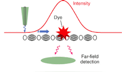
While the SPP effect is well-known in Raman scattering, researchers at the California Institute of Technology (Caltech; Pasadena, CA) and the University of Southern California (Los Angeles, CA) have just demonstrated and measured SPP propagation as originally theorized along a closely packed chain of noble-metal nanoparticles (see figure).1, 2
"One way to think of this plasmon effect is that you have an ordered array of metal nanoparticles and each of these particles is an antenna," said lead author and Caltech researcher Stefan Maier, whose work was presented at the April meeting of the Materials Research Society. "So if you can excite one of these particles, you can excite the particle next to it and so on, and propagate energy along the array."
Progressing from a theoretical statement to a measurable demonstration required several steps. The first was a microwave analog, in which a small dipole was used to study the propagation of energy at gigahertz frequenies along an array of copper rods. The next step involved electron-beam lithographic fabrication of gold and silver nanoparticles. Light was shone on all of them simultaneously while the researchers took spectral measurements to determine the coupling strengths between nanoparticles.
Based on this information, they developed an analytical theory that enabled prediction of parameters such as group velocities and energy attenuation distances. The resulting model was confirmed using finite-difference time-domain simulations. The computer model also served to determine an optical nanoparticle geometry, which ultimately consisted of silver rods with dimensions of 90 × 30 × 30 nm and with 50-nm spacing between adjacent nanoparticles.
The experiment consisted of exciting only one particle at various positions in the chain using the tip of a near-field scanning optical microscope and then noting the patterns of propagation, using a small plastic bead filled with fluorescent dyes and placed at varying positions along the nanocrystal chain. They observed signal damping on the order of -3 dB for every 100 nm of energy transport along the waveguide. So distances up to about 500 nm were achieved before the signal decayed below the dark noise level.
This relatively short propagation distance, which Maier thinks might be extended to 1 µm with further development, eliminates the potential of nanoparticle arrays to act as conventional waveguides. They are likely, however, to act as energy concentrators or couplers between nanoparticle signals and conventional waveguides. They may also result in functional nanoscale devices such as switches.
REFERENCES
- S. A. Maier et al., Nature Materials 2, 229 (April 2003).
- J. R. Krenn, Nature Materials 2, 210 (April 2003)

