Newsbreaks
Ytterbium tungstate laser reaches 14 W
Engineers at Spectra-Physics (Mountain View, CA) have achieved record output-power levels from a continuous-wave laser that is based on a ytterbium tungstate (Yb:KGW) laser rod. The device, which has active thermoelectric (TE) cooling of the laser rod, emits a stable 14 W at 1040 nm. In its latest test, the rod was end-pumped with the 60-W fiber-coupled output of two diode bars.
The gain medium delivers a broad bandwidth similar to materials like Ti:sapphire and alexandrite; unlike the latter two gain media, however, Yb:KGW can be directly pumped with laser diodes operating at 940 or 980 nm (Ti:sapphire requires pumping in the visible wavelength range, usually with a more complicated frequency-doubled neodymium-based solid-state laser). The simplest configuration for a diode-pumped Yb:KGW laser is to pump with the fiber-coupled output from one or more diode bars; the thermal management problems that are minimized through TE cooling had previously led to cracking and fractures in the laser rods. The broad bandwidth of Yb:KGW offers potential for modelocked lasers and high-power amplifiers with femtosecond output. Contact Arnd Krueger at [email protected].
Dots-in-a-well detector senses at three IR wavelengths
Researchers at the University of New Mexico (Albuquerque, NM) and Georgia State University (Atlanta, GA) have created a cryogenically cooled three-color indium arsenide/indium gallium arsenide (InAs/InGaAs) quantum-dots-in-a-well photodetector that operates on a well-confined bound-to-bound transition from the dots' ground state to a state in the InGaAs quantum well. The device is sensitive at three peaks—3.8 and 8.5 µm in the mid-IR and 23.2 µm in the longer-wave IR. The mid-IR response is due to bound-to-continuum and bound-to-bound transitions, while the long-wave response is due to intersubband transition between dot levels.
Detectors were made with illuminated diameters ranging from 25 to 300 µm. The InAs dots themselves were 20 to 25 nm in size and 8 to 10 nm high. The long-wave response was observed at temperatures up to 80 K. A bias-dependent activation energy on the order of 100 mV was determined—three times larger than for quantum-well infrared detectors (QWIPs) at comparable wavelengths. Unlike QWIPs, the dots-in-a-well detector allows for normal-incidence absorption, eliminating the need for gratings and optocouplers. Contact Sanjay Krishna at [email protected].
Jet-printed transistor array will become backplane for low-cost displays
Bringing inexpensive web-processed flat-panel displays closer to reality, researchers at Xerox PARC (Palo Alto, CA) have developed the first plastic semiconductor transistor array entirely patterned using jet printing, a process aimed at replacing conventional complex vacuum deposition and photolithographic techniques.
The arrays are printed at 600 dpi or higher on either flexible or rigid substrates. First, polymer inks and other materials are patterned directly onto a substrate, then a mask is jet-printed on top. The inks and other materials are then dissolved away except where protected by the printed mask. The printer is controlled by a vision system to ensure proper alignment of the layers, even if the substrate warps or deforms during processing. "The process is analogous to color registration," says Raj Apte, a research scientist at PARC. "The printer correctly positions each layer of color with respect to the other layers. In this case, the layers to align are metal, dielectric, and semiconductor, which create the transistor arrays." The technique of jet-printing polymer semiconductors builds on the invention of polythiophene-based semiconducting polymer ink at the Xerox Research Centre of Canada (Mississauga, Ontario). Contact Bob Street at [email protected].
Light may hold ball lightning together
Ball lightning has been a mystery throughout the ages, with some people skeptical even of its existence. Photos and many eyewitness accounts, however, verify its existence; the challenge for researchers has been to try to figure out how a plasma could confine itself and hold itself together in the atmosphere for extended periods of time (up to a minute or longer). John Gilman, a professor at the University of California, Los Angeles, believes he has an explanation: photon-exchange forces hold the balls together.
The luminosity of ball lightning indicates that at least some of its particles are Rydberg atoms or molecules (excited to very high quantum states). Typical ball sizes range from 0.02 to 1.5 m; cohesion within a 0.2-m ball occurs as a result of long-range dipole-dipole interactions between Rydberg atoms with principal quantum numbers of up to approximately 104. The polarizability of such atoms is large, and the interaction energy between the atoms scales as the square of the polarizability. Shear modulus is roughly calculated to be 1.4 atm—consistent with the behavior of ball lightning that has been seen to pass through small openings. Contact John Gilman at [email protected].
Near-field photoluminescence spectroscopy provides first exciton mapping
Spatial resolution on the order of 30 nm, achieved with near-field photoluminescence spectroscopy, has enabled researchers in a multi-institutional collaboration led by the Kanagawa Academy of Science and Technology (Kawasaki, Japan) to map out center-of-mass wave functions of excitons (short-lived electron-hole pairs that combine to give off photons) within a gallium arsenide quantum dot. Exceedingly high-resolution was achieved in the near-field scanning optical microscopy technique by using an optical fiber probe with a 20-nm diameter.
The probe transmitted a 633-nm excitation from a He-Ne laser to the sample quantum dot and also collected the resultant photoluminescent signal. Multiple near-field spectral measurements taken in 11-nm steps across the surface area of the sample were used to construct two-dimensional images and to distinguish exciton from biexciton emissions. The experiment substantiates theoretical predictions of a direct connection between the optical local density of states of elementary excitation and the wave function of the exciton. It also introduces a promising new technique for nanoscale imaging. The researchers described the technique as providing a bridge between the nanometer-scale resolution of electron microscopy and the wavelength-resolution of far-field microscopy. Contact Kazunari Matsuda at [email protected].
Quantum-cascade photonic-crystal laser emits vertically
The band structure of a semiconductor laser can be tailored electronically (quantum-cascade lasers) or photonically (photonic-crystal resonant cavities); researchers at Lucent Technologies (Murray Hill, NJ), California Institute of Technology (Pasadena, CA), Harvard University (Cambridge, MA), the New Jersey Nanotechnology Consortium (Murray Hill, NJ), Université Paris-Sud (Orsay, France), and Princeton University (Princeton, NJ) have now combined both techniques in one electrically injected laser. The device, whose top titanium/gold (Ti/Au) contact results in a bound surface-plasmon wave that produces vertical optical confinement, emits light perpendicular to the semiconductor surface.
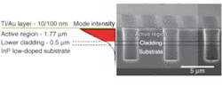
The two-dimensional hexagonal photonic-crystal pattern is etched through the bottom cladding as well as the core, confining light tightly enough that only 10 periods of the photonic lattice are required. Grown on a low-doped indium phosphide substrate, the gain medium is based on a three-well quantum-cascade vertical-transition design emitting at approximately 8 µm. A variety of devices were fabricated with lattice spacings near 3 µm and hole-radius to lattice-spacing ratios of near 0.30. Threshold current density was estimated to be 9 to 10 kA/cm2, a figure that could be improved by fine-tuning the fabrication techniques. The device is potentially useful in quantum optics and as nonlinear photonic-crystal lasers. Contact Raffaele Colombelli at [email protected].
Silica aerogel shows promise for optical power limiting
Silica aerogel is an ideal optical material for nonlinear optical applications such as optical power limiting, say researchers at Hampton University (Hampton, VA), Sogang University (Seoul, Korea), the U.S. Army Research Laboratory (Adelphi, MD), the NASA Langley Research Center (Hampton, VA) and the Korea Research Institute of Standards and Science (Daejon, Korea). One use of optical power limiting would be in maintaining transparency of an optical system for low-power light while attenuating a high-power laser pulse.
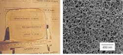
The researchers tested a transparent silica aerogel that had an average pore size of 40 nm, a specific surface area of 780 m2/g, and a density of 0.07 g/cm3 (120-mm piece shown at top; scanning electron micrograph at bottom). The material had a colloidal particle size of roughly 4 nm. The researchers measured the third-order nonlinear refraction coefficient of the aerogel to be approximately -1.5 x 10⁻¹⁵ m2/W—almost five orders of magnitude higher than that of bulk silica. Contact Jae Tae Seo at [email protected].
Subwavelength grating may become variable reflector
Subwavelength gratings are interesting in that they can affect the light passing through them without the creation of diffraction orders; infrared grid polarizers are one example. Now, researchers at Sandia National Laboratories (Albuquerque, MN) have come up with a concept for a subwavelength grating that can drastically vary its reflectance. The device actually comprises two interdigitated gratings: one that moves laterally (for example, using microelectromechanical systems) with respect to the other.
In one example for use with 633-nm light, one grating with a period of 0.6 µm is interdigitated with another. If equispaced, the lines have a period of 0.3 µm, but shifting one grating creates alternating larger and smaller spaces. The researchers performed rigorous coupled-wave analysis on such a structure for different linewidths and grating shifts. For one polarization, reflectance can be varied from 0.85 to zero; reflectance for the other polarization drops to zero at a different wavelength, making possible an effective polarizing beamsplitter. All calculations were done for an amorphous-diamond grating above a silicon substrate, considered realizable by photolithographic techniques. If fabricated, the device could become a low-cost optical modulator or detect subangstrom displacements. Contact Dustin Carr at [email protected].
Ultraviolet LED relies on quantum dots
Quantum dots (QDs) have the potential to replace quantum wells in light-emitting diodes (LEDs), resulting in more-stable spectral output as a function of temperature. Scientists at Hokkaido University (Sapporo, Japan), Nippon EMC (Tokyo, Japan) and Mitsubishi Cable Industries (Hyogo, Japan) have created the first ultraviolet-emitting LED based on QDs. The use of silicon as an antisurfactant prior to QD growth allowed 50-nm gallium nitride QDs to be fabricated on an aluminum gallium nitride (AlGaN) substrate.
The QD density reached 1010 to 1011 cm-2, with dot sizes controlled by adjusting the growth time. The electrically injected devices emitted continuous-wave 360-nm light at room temperature. Contact Satoru Tanaka at [email protected].
Correction
The technology described in the Newsbreak "Liquid-crystal lens focuses electrically" (Aug. 2003, p. 11) was actually previously developed by researchers at the Samara Branch of the Lebedev Physical Institute of the Russian Academy of Sciences and Samara State University (both of Samara, Russia), and the Technical University of Delft and Flexible Optical BV (both of Delft, The Netherlands). The results were published in Optics Letters 23(13), July 1, 1998 (A. F. Naumov et al., "Liquid-crystal adaptive lenses with modal control"). The lens has been fabricated and marketed by Flexible Optical BV since 1997.