'Nano' takes its first real steps into the industrial world
Like many things bearing the prefix "nano," nanomanufacturing—also known as nanofabrication, nanomachining, and nanoprototyping—is pushing the boundaries of what the laser industry has typically considered materials processing. In the process, it is providing some of the first true commercial applications for lasers and optics in the nanoscale realm.
Laser processing is a well-established technique for micromachining, thin-film synthesis, and microdevice prototyping, but it is also showing unique capabilities for nanoscale synthesis and processing of materials. Much of what has been done so far in nanomanufacturing (typically defined as sub-100 nm) leverages existing processes such as photolithography or takes concepts such as laser sintering into new dimensions for applications in microelectronics, optical communications, solar panels, optical storage, biofluidics, and semiconductor manufacturing. At the first symposium on nanomanufacturing held in April at the Massachusetts Institute of Technology (MIT; Cambridge, MA), Bob Doering of Texas Instruments noted that the line between nanoscale manufacturing and current chip-making techniques is "blurry" and that the basic lithographic concepts used in semiconductor manufacturing should carry over to nanomanufacturing—especially with the never-ending push to create smaller and smaller form factors on semiconductor chips and integrated circuits.
In fact, this transition is already happening. Laser nanopatterning and nanolithography by tip-enhanced laser irradiation have been reported on since the late 1990s. By combining laser processing and scanning-probe microscopy, researchers have etched lines with widths as small as 30 nm. In a presentation at the 2nd International Symposium on Laser Precision Microfabrication in January 2002, Yong-Feng Lu of the Data Storage Institute at National University of Singapore (Singapore) noted that the strong near-field effect of this technique can produce etching patterns on various substrates with resolution much smaller than 100 nm and that the method may provide a potential solution for high-density recording, such as producing patterned media.
"The focus is on patterning to carry current lithography approaches to the micro- and nanoscales using long-exposure lasers, such as the excimer, which would be useful for parallel patterning of entire masks at the same time," said Haris Doumanidis, program manager for the National Science Foundation's Nanomanufacturing Program (Arlington, VA). "While the applications of lasers and energy sources in general are for two-dimensional patterning of surfaces to create features with some functionality, this same process can be structured into three dimensions through layering."
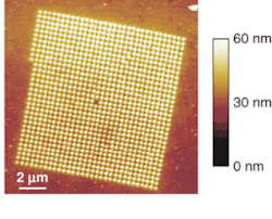
Nanoscale optical lithography techniques are already finding their way into the commercial sector. Engineers at NanoOpto (Somerset, NJ), for example, are using wafer-based nanofabrication techniques to create what the company calls a new class of optical components: nano-optics, which feature physical structures far smaller (less than 250 nm) than the wavelength of light used to create them (see Fig. 1). According to Hubert Kostal, vice president of marketing and sales, the fine-scale surface structures of nano-optics interact with light according to novel physical principles, yielding new arrangements of optical processing functions with greater density and more robust performance. In addition, the small dimensions of nano-optics allow multilayer integration, yielding complex optical components "on a chip" with a broad range of applications and the ability to quickly modify component design, giving a whole new meaning to the concept of rapid prototyping.
"While the optical effects that result when light passes through nanoscale structures have been studied for at least 20 years, cost-effective manufacturing of these optical elements has not been available," Kostal said. "Nanopattern transfer is our proprietary methodology for fabricating optical nanostructures on wafer substrates. Similar to semiconductor fabrication, nanopattern transfer delivers the same commercial benefits: low-cost, high-yield, high-volume production that is easily scaled to demand."
Like its counterparts in semiconductor manufacturing, the nanopattern transfer process involves several steps: constructing a mold inscribed with the complement of the desired nanopattern, transferring the pattern to a resist layer on a prepared substrate, and selectively removing the resist with reactive ion etching to transfer the nanopattern to the target material layer on the substrate. According to the company, various techniques, including holographic lithography and electron beam lithography, can be used to create the desired negative image of a nanostructure.
Nanoscale properties
Another form of optical nanolithography involves the use of a near-field optical microscope (SNOM) to fabricate nanopatterns in photosensitive polymers. Researchers from the University of Cambridge (England), University College London, and the Institute Superior Tecnico (Portugal) have used this approach to obtain features down to 160 nm. The technique involves thin films of a soluble poly(p-phenylene vinylene) (PPV) material, which is exposed to ultraviolet light via the SNOM to make the material insoluble; the material was then washed, dissolving the remaining polymer to create patterns down to 160 nm (see Fig. 2). The patterned polymer is then converted into a fully conjugated PPV by heating it. The result is the fabrication of two-dimensional photonic crystals, which the researchers say could be used in the production of nanoscale photonic devices, integrated electronics, and multicolored displays.
"While we are a long way from micron dimensions, our approach is to go below 100 nm," said Franco Cacialli, department of physics, University College London. "We used an aperture-based SNOM, but an aperture-less SNOM should allow some improvements in resolution. But we believe it is mainly a limitation of the lithographic medium, not the instrument, so we are working with chemists to see if we can get a material with smaller molecular weight that could be used in conjunction with visible light, as opposed to ultraviolet light, to achieve smaller (less than 100 nm) features."
Many nano-based R&D efforts are recognizing that, as with many laser-based applications, the materials being manipulated are a critical consideration in the choice and design of the instrumentation. According to The Freedonia Group (Cleveland, OH), the development of nanoscale materials (substances with particle size between 1 and 100 nm) is a key step in the eventual production of more-sophisticated nanomachines, nanoelectronics, and nanomedical devices (see "Nanotechnology investment targets practical applications," [below])
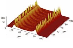
In line with this trend, researchers at the University of California-Berkeley have developed a laser approach for curing 0f gold nanoparticles that saves time and money in the production of integrated circuits. Using an argon-ion laser in conjunction with drop-on-demand ink-jet technology to deposit liquified gold on a substrate, Costas Grigoropoulos and colleagues in the mechanical engineering department at the University of California-Berkeley, have demonstrated the ability to print two-dimensional micropatterns on thin films in about 5 min (see Fig. 3). The nanoparticles are suspended in a solvent and directly heated by the laser; as the solvent evaporates, molten gold nanoparticles agglomerate, resulting in the formation of a continuous gold line. The radiation of the argon-ion laser at 488 nm was shown to be entirely absorbed within a depth of about 1 um below the surface of the gold nanoparticle solution.
According to Grigoropoulous, working with nanoparticle suspensions offers many advantages compared to conventional subtractive integrated circuit processes, including saving expensive materials by depositing material only at desired places on a substrate and working with gold at room temperature rather than in a molten state.
"The thing you can't forget is that the properties of the nanoscale, such as the melting point and boundaries between phase transformation, are different," Grigoropoulos said. "The research we have been pursuing is on the lower melting point of metal nanoparticles, which will enable the sintering of these nanoparticles and. the writing of electronic conducting patterns at temperatures that are relatively low and compatible with plastic substrates."
Overcoming diffraction limits
Not everyone is convinced, however, that lasers are the best way to go when it comes to nanofabrication of polymers, metals, or other materials. In addition to what actually defines "nano," most arguments against the practical viability of laser-based nanoprocessing center on a single issue: diffraction limits.
"The diffraction limit of light limits the size scale on which you can modify materials," said Harold Craighead, professor of applied and engineering physics and codirector of the Nanobiotechnology Center at Cornell University (Ithaca, NY). "So for the same reason that optical microscopes are limited by light, modifying materials have the same restriction. This is why we use electron beams that can be focused to a fraction of a nanometer and so modify materials at several nanometers smaller than with a laser."
While those in the pro-laser camp agree that diffraction limits are an issue at the nanoscale, they disagree that this means lasers are not suited to nanoprocessing.
"The main issue with using laser energy for processing at the nanoscale is diffraction limits," Doumanidis said. "The wavelength is usually at 100 µm of scale, which is too large for processing at the nanoscale. But we are coming up with new ways to work around this problem, such as near-field optics, multiphoton techniques, and plasmonic patterning."
Nanotechnology investment targets practical applications
Despite some overhype in the last few years, investment in nano technologies and applications continues to grow. For example, through its National Nanotechnology Initiative, the U.S. National Science Foundation (NSF) has spent more than $600 million to support R&D in this field since 1997. In addition, the NSF's Nanomanufacturing Program will spend $22 million this year to support fundamental research into the adaptation of technologies such as laser plasma vaporization, laser-guided particle transport, and laser tweezers for practical applications at the nanoscale.
Such commitment appears to be paying off. According to a report published in July by The Freedonia Group (Cleveland, OH), an industrial market research firm, after a decade-long buildup, nanotechnology is beginning to see its first commercial successes. The Freedonia Group expects the U.S. market for nanomaterials (which totaled only $125 million in 2000) to surpass $1 billion in 2007 and reach $35 billion by 2020, with early growth coming from niche applications in manufacturing.
These applications include wafer-polishing abrasives and high-density data-storage media for electronics; improved diagnostic aids for the medical community; transparent sunscreens, stain-resistant pants, and wear-resistant flooring for consumers; cost-cutting equipment coatings for the defense industry; fuel-saving components for the auto industry; and better paper and ink for the printing industry. In the long run, however, The Freedonia Group believes the best opportunities are in health care and electronics, which together should account for nearly two-thirds of the market by 2020.