Nonlinear materials extend the range of high-power lasers
F. KENNETH HOPKINS
Nonlinear optical (NLO) materials can significantly enhance laser performance by enabling wavelength shifting and tunability over a broad spectral range. Technical progress has been made in developing several crystals that together cover the spectral range from mid-ultraviolet to the far-infrared. Systems incorporating zinc germanium phosphide (ZGP), for example, have already demonstrated tunability over much of the mid-infrared atmospheric window, with an average power of approximately 3.5 W. Significant improvements have also been made in extending the transparency range and improving the laser-damage resistance of the potassium titanyl phosphate (KTP) family of compounds.
Some of the multitude of applications requiring use of NLO elements in laser systems include military infrared countermeasures, environmental monitoring by differential absorption laser radar operating in the 2- to 14-µm wavelength range, windshear detection, medical diagnosis and treatment, materials processing, scientific instruments, optical communications, low-light imaging, atmospheric aberration compensation for astronomy and satellite tracking, scene projectors, optical signal processing, data storage, underwater communications and imaging, and remote identification of biological materials. However, available nonlinear optical materials have been unsatisfactory for many applications due to small nonlinearities, poor optical clarity, small thermal conductivities, difficulty in processing into devices, and other factors.
Wright Laboratory program
The Air Force Wright Laboratory has been the primary Department of Defense organization behind the development of new NLO crystals for laser systems. The Air Force’s Wright Laboratory Materials Directorate (WL/ML) is developing improved NLO materials for laser sources capable of generating tens of watts of average power over the extensive wavelength range from the mid-ultraviolet to the far infrared, but the greatest emphasis is being placed on the infrared spectral region. Current research and development is focused on far-infrared conversion materials, semiorganics, borates, zinc germanium phosphide, and potassium titanyl phosphate and its isomorphs (see Fig. 1).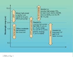
Far-infrared conversion materials are needed to shift the high optical power available from CO2 lasers into the mid-infrared region and to provide wavelength-tunable laser light over the far-infrared atmospheric window. Currently available materials—ZGP, silver gallium selenide (AgGaSe2), and thallium arsenic selenide (TAS)—limit average conversion powers to a few watts. For ZGP, the limitation is due to optical absorption properties and to a less than ideal orientation angle that results in a reduced effective nonlinear coefficient.
AgGaSe2 is principally limited by a low thermal conductivity. AgGaSe2 and TAS have only moderately sized nonlinear coefficients, less than one third of that of ZGP. In addition, TAS is a relatively soft, brittle material with a low melting temperature (3°C), characteristics that severely complicate the fabrication of high-quality surfaces and surface coatings, and it has a low thermal conductivity and a moderately large walkoff angle.
A number of candidate materials are being investigated for the far-infrared region. The most promising are cadmium germanium arsenide (CdGeAs2), gallium selenide (GaSe), and quasi-phase-matched semiconductor structures. CdGeAs2 offers an enormous nonlinearity (d36 = 235 pm/V), a wide transparency range (2.3–17 µm), and a moderately large birefringence (0.096), resulting in an enormous figure of merit (d2/n3 = 1288 pm2/V2).
Future work is aimed at developing a technique to grow large crystals with a reduced absorption shoulder at shorter wavelengths. This absorption is due to crystal point defects, a common problem for chalcopyrite semiconductor crystals. The second candidate, GaSe, has a large figure of merit (d2/n3 = 214 pm2/V2) for this spectral region. However, the growth of high-quality GaSe crystals will be difficult because, like mica, they are weakly bonded in the c-direction. Alloying may overcome this limitation.
Another category, quasi-phase-matched semiconductor structures, is making use of the large nonlinear coefficients of well-developed semiconductors such as gallium arsenide. The recent development of diffusion bonding techniques has made these structures possible.
Semiorganics combine the high optical nonlinearity of organics with the physical ruggedness of inorganics. Many of the candidates in this category are intrinsically low cost because they can be aqueously grown, either in the form of an organic/inorganic salt or an organic ligand/metal-ion complex. They are useful in the near-infrared and visible spectral regions.
The two most important of these materials to date are deuterated thiosemicarbazide cadmium chloride (d-TSCCC) and deuterated cadmium triallylthiourea chloride (d-CAT). Compared with other known materials, these crystals have among the best figures of merit for type-II third-harmonic generation of 1064 nm (Nd:YAG); for second-harmonic generation of 972 nm, a Fraunhofer line that is an efficient seawater transmission wavelength; and for the second-harmonic generation of 868 nm, another Fraunhofer line.
Borate crystals offer the possibility of highly efficient ultraviolet laser sources that are all-solid-state. For example, a laser source using lithium triborate (LiB3O5 or simply LBO) operating at 289 nm and pumped at 1064 nm by a Nd:YAG laser recently demonstrated an overall optical efficiency of 25%.1 Patents for LBO growth are currently held by the Chinese. Continuing problems with LBO, such as long delays in receiving crystals and poor-quality crystals due to flux inclusions, appear to still exist, limiting its applications and availability. It is also reported that China has no interest in licensing the growth to US crystal growers. New borate compounds not patented by Chinese researchers are being investigated that will permit conversion deeper into the ultraviolet spectral region.
Zinc germanium phosphide
The development of zinc germanium phosphide is the most important success resulting from the WL/ML program. First explored in the late 1960s and early 1970s, ZGP was the focus of a renewed research and development effort in the late 1980s due to its high nonlinear coefficient, wide transparency range, wide phase-matching range, good mechanical properties, and good thermal properties.
AgGaSe2 has been the only serious competitor to ZGP for 2-µm-pumped optical parametric oscillator (OPO) applications. However, the material is intrinsically limited to low-average-power operation due to a low thermal conductivity that leads to a thermal gradient and subsequent thermal lensing.2
With AgGaSe2 thus largely discredited for higher-power, mid-IR applications, ZGP is now the material of choice for 2-µm-pumped OPOs with average powers greater than 1 W. In addition, it has often been used for frequency doubling the shorter CO2-laser wavelengths having lower power. Four factors contributed to the success of the early-development programs: the development of innovative compound synthesis and crystal growth methods, crystal defect analysis and identification, the development of advanced processing techniques, and device demonstration and evaluation.
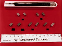
ZGP single crystals are grown using a two-stage process. First, elemental zinc, germanium, and red phosphorus are placed in boats, sealed into heavy-walled quartz ampoules, and heated to form single-phase ZGP. A heating cycle ensures the completion of intermediate reactions, avoiding excessive pressure build-up due to free phosphorus and zinc. Single crystals are then grown using the seeded horizontal gradient freeze technique, which results in unidirectional solidification by cooling the material in the presence of a controlled thermal gradient in a two-zone horizontal-growth furnace. The technique has been successful in growing single crystal boules with extremely low thermal gradients and minimized stress across the boule (see photo at top of this page).3
To improve crystal yield and reduce production time, two innovative techniques have been developed. The first, the use of a high-temperature transparent furnace, allows visual monitoring of the growing crystal and prevents seed loss due to melt-back in this very-low-gradient environment (see Fig. 2). If twinning occurs, the twinned portion can be melted back and single-crystal growth reinitiated. The elimination of seed meltback and twinning has resulted in impressive yield gains. The second innovation, now being further refined, is the rapid synthesis of ZGP by phosphorus injection.4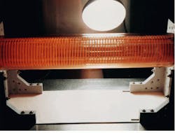
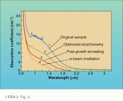
After an extensive analysis effort including transmission spectroscopy, photoluminescence, Hall measurements, electron paramagnetic resonance (EPR), cathodal luminescence, electron nuclear double resonance, optical EPR, and magic-angle-spinning nuclear magnetic resonance, the defect was found to be due to a native acceptor rather than impurities. Early characterization indicated that the acceptor is deep, highly polarization sensitive, and caused by a zinc vacancy or a zinc ion on a germanium site. Recent studies have identified the defect as the zinc vacancy, and show no evidence of disorder or non-stoichiometric-related antisites. Even in zinc-rich material it appears that a zinc-rich cubic phase of Zn3P2 forms dilutely, still allowing zinc vacancies to remain the dominant defect. Subsequently, photoinduced EPR has identified that the phosphorus vacancy is the dominant donor in this highly compensated material.
Partially guided by the defect analysis efforts, processing methods developed during the ZGP program were significant factors in its success. Thermal annealing and radiation treatment procedures improved transparency, probably due either to a reduction in zinc vacancies or to an introduction of phosphorus vacancies. Electron-beam and gamma-ray irradiation of crystals appears to create donor sites deeper in the energy gap that compensate for the native acceptors. Another area of enhanced processing concerns improvements to surface finishing and antireflective-coating techniques.
The fourth facet of the ZGP success was the demonstration of the material in OPOs, validating the success of the program and providing guidance to the materials research and development effort. An OPO using ZGP produced an output of more than 2.5 W at a frequency of 4 kHz, a pump wavelength of 2.05 µm, output efficiencies of almost 50% overall, and a slope efficiency of approximately 68% (see Fig. 4).5 More-recent demonstrations have yielded approximately 3.5 W of output power. Due to the large thermal conductivity of ZGP, the absorption coefficient in these tests was 0.26/cm at 2.05 µm, significantly larger than that of AgGaSe2. A rollover appearing in the plot of output power as a function of pump power is believed to be due to signal reconversion rather than thermal effects.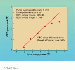
Future development of ZGP will focus on establishing a reliable process that produces large single crystals with high transparency (<0.15/cm at 2.05 µm) and a high degree of homogeneity.
Potassium titanyl phosphate
The final category of nonlinear materials is the potassium titanyl phosphate family of compounds. KTP has high nonlinear optical coefficients, a high optical damage threshold, wide acceptance angles, and thermally stable phase-matching properties that make it useful for high-power wavelength-conversion applications such as second-harmonic generation and OPOs.6 Large, linear electro-optic coefficients and low dielectric constants make it attractive for other applications such as modulators and Q-switches. Until recently, the application and availability of the crystal have been limited, in part due to a series of patents held by DuPont, now expiring.
Wright Laboratory pushed the state of the art for KTP crystal growth, developing both the flux and hydrothermal growth techniques.7-9 Current R&D programs are focusing on three areas: the exploration and early development of KTP isomorphs that extend useable wavelength range beyond 5 µm, the growth of KTP with a reduced susceptibility to gray tracking, and the exploration and early development of KTP alloys that permit noncritical phase matching at selected wavelengths. Wright Laboratory is principally pursuing the first two areas.
KTP is limited to wavelengths below 3 µm for high-power applications, leading to development of KTP isomorphs. The most promising candidates to date are KTiOAsO4 (KTA), RbTiOAsO4 (RTA), and CsTiOAsO4 (CTA), materials with extended wavelength ranges permitting the high power from Nd:YAG at 1 µm to be converted to wavelengths as long as 5 µm (see Fig. 5). In addition, due to a low electrical conductivity, they can provide improved Q-switches for the mid-infrared. However, even these may be limited to lower output power because the arsenate compounds are characterized by small absorption in the 4- to 5-µm range. Therefore, other KTP-like compounds are being investigated.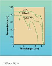
In addition to the wavelength limitations of KTP, laser damage caused by a defect referred to as gray tracks has limited the use of the material in laser systems with high average power. From an investigation of the causes for the gray-track effect and its relationship to the chemistry and crystal growth processes, an improved crystal growth technique has been developed that reliably produces economical, large-aperture crystals with significantly improved damage thresholds. In fact, a standardized laser test system capable of inducing damage in all other types of commercially available KTP could not damage the new material, even using 10,000 shots of 20-ns pulses at a wavelength of 532 nm and a power density of 3 J/cm2.10 This breakthrough should lead to the availability of low-cost, large-aperture KTP from Crystal Associates (Waldwick, NJ) with a greatly improved damage threshold.
Nonlinear optical crystals are needed for laser sources that are in turn required for a number of applications. As a result of Wright Laboratory’s NLO materials program, crystals with greatly enhanced properties are beginning to make these applications possible.
REFERENCES
1. Alex Kaz and Larry Marshall, post-deadline paper #CFF4 at CLEO, May 1994.
2. C. L. Marquardt et al.; Appl. Opt. 33, 3192 (20 May 1994).
3. Peter Schunemann, MRS 1993 Fall Meeting, 29 November 1993, Paper #R1.4.
4. David F. Bliss et al., Crystal Growth 137, 145 (1994).
5. M. G. Knights et al., OSA Advanced Solid-State Lasers Meeting, 7 February 1994, Paper #AWD4.
6. L. K. Cheng and J. D. Bierlein, Ferroelectrics 142, 209 (1993).
7. G. M Loiacono and R. A. Stolzenberger, Air Force Technical Report AFWAL-TR-89-5001.
8. R. F. Belt et al., Air Force Technical Report AFWAL-TR-84-1074.
9. T. E. Gier and F. C. Zumsteg, Air Force Technical Report AFWAL-TR-78-208.
10. M. P. Scripsick et al., Advanced Solid State Lasers Conference 1995, Memphis, TN, Paper #PD-17.
ACKNOWLEDGMENTS
I acknowledge the many scientists and engineers whose inspired efforts have made this program a success, among them Mel Ohmer, Nils Fernelius, David Zelmon, Uma Ramabadran, and David Fischer from WL/ML; David Bliss from AF Rome Lab; Peter Drevinsky from AF Phillips Lab; Margaret Rakowsky from AF Seiler Lab; Tom Pollak and Peter Schunemann from Lockheed Sanders; Gabe Loiacono, Dick Stolzenberger, and Dominic Loiacono from Crystal Associates; Gretchen Kennedy and Gary Catella from Cleveland Crystals; and Narsingh Singh from Westinghouse.
F. Kenneth Hopkins is the Direction Leader for Nonlinear Optical Materials, Wright Laboratory Materials Directorate (WL/MLPO),Wright Patterson Air Force Base, OH 45433-7707.