IMAGING MICROSCOPY: Hybrid microscope probes plasmonic nanostructures
Researchers at JILA, a joint institute of the National Institute of Standards and Technology (NIST; Boulder, CO) and the University of Colorado (Boulder), are developing a method of imaging nanostructures that is intended to enhance and complement existing microscopy techniques; it does this by combining diffraction-limited optical excitation with detection of photons and low-kinetic-energy photoelectrons.1
The researchers ultimately hope to combine confocal-fluorescence or Raman spectroscopy with time-resolved photoelectron imaging spectroscopy for applications such as the investigation of local plasmonic effects in nanostructures. So far, they have demonstrated a scanning-photoionization microscopy (SPIM) technique that could, in principle, yield spectroscopic information in thin nano- and mesostructured polycrystalline metal patterns, spatially resolved down to the single-molecule level.
Their experimental apparatus enables simultaneous measurement of optical-penetration depth and two-photon photoemission cross section from a diffraction-limited spot size in a photolithographically patterned polycrystalline gold film placed on a glass cover slip. Comparison of these measurements with atomic-force-microscopy scans indicates that photoionization contrast varies as a function of electron escape depths and thickness variations across the sample. The researchers also implemented a simple form of spatially resolved photoemission spectroscopy, which they expect to enhance using time-of-flight electron-energy analysis.
Ti:sapphire light source
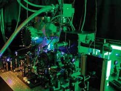
The light source in their scanning-photoionization microscopy setup was a Kerr-lens passively modelocked Ti:sapphire oscillator driven by a frequency-doubled diode-pumped solid-state Nd:YVO4 (vanadate) pump laser. Frequency doubling and dispersion compensation yielded 415 nm, 100 fs pulses with 0.18 nJ pulse energies, which were focused to a near-diffraction-limited spot at the sample by a Schwarzschild-type reflective microscope objective. The sample was scanned over the stationary laser beam using a combination of independently operated coarse and fine translation stages (see Fig. 1).
The researchers performed fluorescence measurements by collecting red-shifted photons with the microscope objective and focusing them through a confocal pinhole into a single-photon-counting photomultiplier module, enabling subsequent generation of confocal-microscopy images. In addition, multiphoton absorption enabled photoionization imaging using a Faraday cup that collected photoelectrons to produce a photocurrent, which the researchers measured using a picoammeter as a transimpedance amplifier. Electron kinetic-energy distributions were also obtained by slowly varying the Faraday-cup bias.
The researchers observed photoemission at three distinct intensity levels: zero detectable photocurrent from the glass cover slip (a wide-band-gap insulator), a small but finite photocurrent from the solid parts in the polycrystalline thin metal film, and strong photoemission at the metal film edges (see Fig. 2).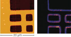
The combination of high detection sensitivity, structural information, and strong surface specificity makes developing chemically sensitive photoelectron spectroscopy with high spatial and temporal resolutions particularly desirable for investigating heterogeneous nanostructured materials as well as surface-enhanced Raman scattering (SERS)-active nanoparticles in complex environments, such as on electrode sensors or thin films.
“The method is in its infancy, but nevertheless it does have the power to provide a new set of eyes for looking at nanostructured metals and semiconductors,” said David Nesbitt, who leads the research group. The group is currently investigating the even more interesting possibility of mapping out plasmonic contributions to photoemission spectroscopy explicitly in the frequency domain by tuning the system over a series of excitation wavelengths. The research is supported by the Air Force Office of Scientific Research (Arlington, VA) and the National Science Foundation (Arlington, VA).
REFERENCE
1. O.L.A. Monti et al., J. Chemical Physics 125, 154709 (Oct. 21, 2006).
About the Author
Hassaun A. Jones-Bey
Senior Editor and Freelance Writer
Hassaun A. Jones-Bey was a senior editor and then freelance writer for Laser Focus World.