SILICON LASERS: Intel and UCSB create first modelocked silicon laser
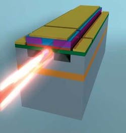
The past few years have seen the watershed advance of electrically pumped silicon lasers (see www.laserfocusworld.com/articles/274700). Now, a team at the University of California-Santa Barbara (UCSB; Santa Barbara, CA) and Intel (Jerusalem, Israel), led by John Bowers at UCSB, has expanded on this work to accomplish modelocked, evanescent-silicon-laser transmission with 40 GHz repetition rates.1 This first-ever milestone in silicon matches rates achieved in other media, but promises a significantly lower cost and power consumption than other devices, as well as a more compact footprint (see Fig. 1).
Modelocked evanescent lasers deliver short, stable pulses of light, making them useful transmitters when combined with data-encoding modulators. In this new laser, pulses that repeat 40 billion times per second are composed of many evenly spaced wavelengths of IR laser light that could be used in wavelength-division multiplexing or multiple wavelength generation, replacing hundreds of lasers with one.
Silicon doesn’t generate a current when subjected to an applied voltage like III-V materials. So the UCSB team created a hybrid silicon/III-V platform by transferring thin layers of conductive indium phosphide (a III-V material) to a 2.5 × 0.69 µm silicon waveguide using low-temperature wafer bonding. The laser had a cavity length of 1060 µm and an absorber length of 50 µm.
Lasing occurred at a threshold current of 196 mA, but passive modelocking occurred at 206 mA and an absorber bias of 0.4 V, resulting in an average fiber-coupled output power of -3 dBm. The forward-biased absorber generated a photocurrent of 1.15 mA. Using high-reflectivity coatings on the facets and shorter gain sections integrated with passive-waveguide sections would improve the modelocked lasing threshold, say the researchers. Optimizing aspects of the fabrication should further improve injection efficiency to enable thresholds below 20 mA.
The pulses had a 4.2 ps intensity pulse width, and a spectral width of 0.9 nm with modes spaced every 0.33 nm (see Fig. 2). The lasers have low jitter and extinction ratios above 18 dB.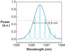
The fabrication of these devices includes dicing the chips and polishing the edges to extract light from the laser, an imprecise process that also defines the cavity length. The next step in their work, says Brian Koch, UCSB graduate researcher, is to use a more precise photolithography process to form the laser cavity. High precision in the cavity length allows a precisely determined repetition rate, essential when designing optical transmitters for a specific data rate, says Koch.
The potential applications for modelocked silicon lasers are numerous, including optical-clock signal generation, light detection and ranging, clock recovery, and coherent communications systems. “The most exciting thing about these lasers,” says Koch, “is the prospect of completely new types of integrated technology.”
REFERENCE
1. B. Koch et al., Optics Express 15(18), 11225 (Sept. 3, 2007).
About the Author

Valerie Coffey-Rosich
Contributing Editor
Valerie Coffey-Rosich is a freelance science and technology writer and editor and a contributing editor for Laser Focus World; she previously served as an Associate Technical Editor (2000-2003) and a Senior Technical Editor (2007-2008) for Laser Focus World.
Valerie holds a BS in physics from the University of Nevada, Reno, and an MA in astronomy from Boston University. She specializes in editing and writing about optics, photonics, astronomy, and physics in academic, reference, and business-to-business publications. In addition to Laser Focus World, her work has appeared online and in print for clients such as the American Institute of Physics, American Heritage Dictionary, BioPhotonics, Encyclopedia Britannica, EuroPhotonics, the Optical Society of America, Photonics Focus, Photonics Spectra, Sky & Telescope, and many others. She is based in Palm Springs, California.