Nanospikes add new functionality

Dec. 1, 2007
By creating “nanospikes”-nano- and microsize hills and valleys-on the surface of metals and semiconductors, researchers at the University of Virginia (Charlottesville, VA) expect that the increased surface-area of the materials could, for example, increase the absorption of light for optoelectronic sensor and solar-energy applications, improve cell growth and integration of metal-coated hip or joint implants, or dissipate heat more efficiently in computer chips.

By creating “nanospikes”-nano- and microsize hills and valleys-on the surface of metals and semiconductors, researchers at the University of Virginia (Charlottesville, VA) expect that the increased surface-area of the materials could, for example, increase the absorption of light for optoelectronic sensor and solar-energy applications, improve cell growth and integration of metal-coated hip or joint implants, or dissipate heat more efficiently in computer chips.

Click here to enlarge image

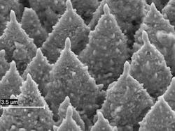
Initial nanospike experiments used undoped germanium wafers exposed to 130 fs, 1.4 mJ pulses at 800 nm with a repetition rate of 1 kHz from a regeneratively amplified Ti:sapphire laser system. Very sharp conical microstructures with nanospikes atop are formed when the sample is scanned under the laser beam (fluence approximately 0.6 J/cm2). The resulting microstructures are 10 to 15 µm tall, with a base diameter around 5 μm tapering down to approximately 100 nm near the tip, and are formed spontaneously in a self-assembled manner inside the laser spot. The spike formation is dependent on laser fluence and number of shots. In addition to nanospikes in germanium and other semiconductors, the team has successfully textured metals like titanium and stainless steel. Contact Mool Gupta at [email protected].

Sponsored Recommendations

On demand webinar: Meet BMF’s first hybrid resolution printer, the microArch D1025

July 26, 2024
Join us in this webinar to explore our newest product release - the microArch D1025 - our first dual-resolution printer. Learn more!

Meet the microArch D1025: Hybrid Resolution 3D Printing Technology

July 26, 2024
Meet BMF's newest release, our first dual-resolution printer for the prototyping and production of parts requiring micron-level precision.

Optical Power Meters for Diverse Applications

April 30, 2024
Bench-top single channel to multichannel power meters, Santec has the power measurement platforms to meet your requirements.

Request a quote: Micro 3D Printed Part or microArch micro-precision 3D printers

April 11, 2024
See the results for yourself! We'll print a benchmark part so that you can assess our quality. Just send us your file and we'll get to work.

Voice your opinion!

To join the conversation, and become an exclusive member of Laser Focus World, create an account today!