Optoelectronics World News
Laser ablation powers plane
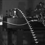
Scientists at the Tokyo Institute of Technology (Tokyo, Japan) have accomplished the first flight of airplanes driven by a laser. Even though the targets were several centimeters long, made of paper, and weighed tenths of a gram, the significance is no less exciting (see figure).
"If our findings are correct," said Takashi Yabe, professor of mechanical engineering, "a ten-ton airplane could be accelerated using a 1-Hz, 100-kJ laser." A 100-kJ laser already exists, added Yabe, and Lawrence Livermore National Laboratory is building a 1-MJ laser (for the purpose of laser-driven fusion). A laser repetition rate of 1-Hz is a possibility in the near future.
Perhaps surprisingly, the successful fuel for the laser-ablation experiment was found to be water rather than solid substances or gases. A single 5-ns pulse of a 1064-nm-emitting Nd:YAG laser onto an aluminum-foil target with a 0.014-g droplet of water generated enough impulse to propel the plane up to 1.4 m/s. But further modeling showed that a layered target would better focus the ejected atoms to impart a greater momentum to the plane. The maximum value of 104 Näs/MJ obtained by the experiment means that one pulse of a 1-MJ laser could give a velocity of 1 m/s to a 10-ton airplane. After 300 pulses it would reach the speed of sound. Thus, smaller lasers would be sufficient for practical applications such as airplanes and ships.
The idea of using laser ablation to propel craft has been around for decades, but generally using a solid propellant.2 In this demonstration, water generated greater thrust than a thin coating of acrylic, but such a configuration does not lend itself to repetitive acceleration after the propellant is used up. One solution is using water vapor from the atmosphere to continually refresh the configuration. Because jets suck in tons of air during a trip, humidity high in the atmosphere may be a practical source of water, says Yabe.
Alternately, water can be supplied on the structure. A water supply demonstrated by the researchers contains water between two plates with a 2-mm hole in one side. Surface tension keeps the water from escaping and quickly resupplies it after irradiation.
Tracking Technology
The second practical problem with laser propulsion is tracking the moving target with the laser. The National Space Development Agency of Japan is testing acquisition and tracking technology for laser intersatellite communications that could be applicable in the case of laser-propelled aircraft. The Optical Inter-Orbit Communications Engineering Test Satellite aims to demonstrate pointing, acquisition, and tracking technology. With a water supply composed of many holes, the exact location of the hole is not necessarily illuminated.
Yabe has more recently succeeded in moving a miniature bus that was 7 cm long and weighed 10 g, nearly 100 times heavier that the micro- airplane. Because the bus moved on wheels, the friction from the "ground" is minimized.
The group is planning to fly and control a larger airplane using a larger laser in collaboration with the National Laboratories of Japan. If practical systems are successful, said Yabe, high-altitude flight could be enabled in the stratosphere where jet engines cannot be used. A flight between Tokyo and New York on such a craft could conceivably be completed in three hours.
Many other applications are seen, including a nanomachine propelled by a low-intensity x-ray source that can move through a blood vessel to aid in disease diagnosis. In addition to alternative propulsion for space vehicles, the concept can be used for environmental observation of volcanoes or the climate by kite-plane. Another project involves hoisting airships above Japan to act as telecommunication relay stations that are less expensive than launching a satellite.
A micro-airplane with a water droplet overlay, imaged in motion by a high speed-camera, is launched by a pulsed Nd:YAG laser.
Valerie C. Coffey
REFERENCES
- T. Yabe et al., Appl. Phys. Lett. 80, 4318 (2002).
- T. Yabe et al., invited paper, SPIE Conf. on High Power Laser Ablation, Taos, NM (2002).
Hollow waveguide clips femtosecond pulse wings
One of the main problems to overcome in developing the next generation of hundred-terawatt and one-petawatt laser systems will be to produce very short and clean pulses that have clean shapes with no wings or pedestals, according to Alexander Gaeta at Cornell University (Ithaca, NY). A team of researchers from Cornell and the University of Michigan (Ann Arbor) presented a potential solution to this problem last May during the Postdeadline Paper session at CLEO 2002 (Long Beach, CA).
The problem is of most concern just after the first stage of amplification in amplified femtosecond laser systems, in which amplified spontaneous emission can carry a significant wallop even if it is several orders of magnitude below a main pulse with a petawatt peak.
FIGURE 1. In an experimental scheme for pulse-contrast enhancement of high-energy laser pulses, a linearly polarized, high-energy pulse with a small pre-pulse is elliptically polarized. It is then coupled into a noble-gas-filled hollow waveguide where only the high-intensity portion of the beam undergoes nonlinear ellipse rotation. At the output end, the polarization of the low-intensity pre-pulse is returned to its initial polarization and is rejected by a polarizing beam-splitter while the high-intensity part of the beam is transmitted by the beamsplitter.
"People are interested in looking at light-matter interactions at intensities of 1021 or 1022 W/cm2, and it turns out that you ionize the electrons in most matter, whether solid, gas or liquid, at about 1014 W/cm2," Gaeta said. "So if you do the math you can see that pedestals, even a factor of 108 below the peak of the main pulses, will still ionize the material. Then the interaction is no longer with a neutral atom or a neutral solid, but with a plasma, because all of the electrons will be ionized by the pedestal before the main pulse gets there."
Filtering the pedestals out of short pulses on these femtosecond time scales requires a passive method such as nonlinear optics, but methods proposed to date have relied on bulk nonlinear media that do not allow cleanup of pulses that exceed the peak power for self-focusing.
"You can do this in a single-mode fiber," Gaeta said. "The problem is of course that it only works for pulses that are maybe tens of nanojoules at most." After amplification, however, pulse energies enter the microjoule to millijoule regime, and powers range from gigawatts to tens of gigawatts.
Gaeta's team found the first step toward a solution in published research indicating that a gas-filled hollow waveguide could boost peak self-focusing power levels well above the limitations of bulk nonlinear media. "A hollow gas-filled waveguide can propagate a nice clean mode over a distance of about 40 to 50 cm and this has been done by other people," Gaeta said. "By guiding a small beam diameter (on the order of 100 æm) over a relatively long distance you can keep the intensity high but still get a relatively long nonlinear path length. The end result is that you can operate below the critical power for self-focusing, but you can get effectively a pretty large nonlinear effect."
To enhance pulse contrast, the researchers turned to nonlinear ellipse rotation, in which an elliptically polarized beam is propagated through an isotropic material. The ellipse maintains its shape but rotates continuously while propagating. In the time domain, the amount of ellipse rotation depends on intensity, so the peak of the main pulse experiences the most rotation, while the much-lower-intensity pulse wings will undergo little or no rotation.
The experimental setup, which allowed the researchers to diminish pedestal intensities by three orders of magnitude, used quarter-wave waveplates to generate the elliptic rotation prior to propagation through the waveguide and then to undo the polarization afterwards (see Fig. 1). In effect the setup acts like a nonlinear switch, in which a beam splitter at the output with a polarization perpendicular to the input beam passes only the peak pulse signal that underwent the most significant elliptical rotation in the waveguide.
The researchers also placed a compressor at the output of the system to compensate for self-phase modulation, a scalar process in which the time dependency of the index of refraction broadens the pulse spectrum as it propagates through the waveguide (see Fig. 2).
"The broader the spectrum is, the shorter the pulses can be," Gaeta said. "And we find that after propagating through our system the pulses actually remain about the same duration but the spectrum is broadened by about a factor of three due to self-phase modulation." So placing gratings at the output to compress the signal enables the researchers to get output pulses about a factor of three shorter than the input pulses.
Currently, the process is not 100% efficient, however. Only about 15% to 20% of the total input power makes it through the system. One thousand-fold pedestal reduction makes the system useful as is, but increasing efficiency is a primary focus of continued research.
"This is a new way of doing pulse cleanup in pulses from the regime of a microjoule to a millijoule," Gaeta said. "We are also looking at other techniques or modifications of this technique that would allow us to perhaps go up to the joule regime."
null
Hassaun A. Jones-Bey
REFERENCE
1.D. Homoelle, M. Foster, A. L. Gaeta, et al. CLEO 2002, Postdeadline Paper CPDA4:1-3 (May 2001).
LIGHTING OLEDs and phosphors make light together
Although it will take many years for their impact to be felt (or, more precisely, seen), light-emitting diodes (LEDs) designed for illumination will one day begin to gobble up territory now held by incandescent and fluorescent lighting. Such an invasion will occur only when the ruggedness, long lifetime, and potentially higher efficiency of LEDs are not fatally offset by their high cost. Today's LEDs intended for lighting are small, discrete units made possible by gallium nitride (GaN) semiconductor technology; white light is typically created by a broadband phosphor excited by the LED's blue or ultraviolet emission. Although efforts are ongoing to reduce the cost of GaN-based devices, white-light LEDs have so far made their appearance in everyday life mainly in the form of tiny flashlights. Researchers at General Electric (GE; Niskayuna, NY) are aiming to change this situation by changing the basic make-up of the short-wavelength LED emitter.
The GE effort is centered on organic LEDs (OLEDs). Although blue-emitting OLEDs are not new, the researchers plan to combine them with phosphors and boost their combined efficiency to practical levels, making possible the production of large, inexpensive illumination panels. They have constructed an experimental device that not only emits high-quality white light, but exhibits an overall power efficiency increase over the bare blue emitter.1
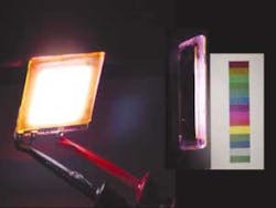
A polymer-based OLED was deposited on one side of a glass substrate, covering an area of 6.35 cm2, then a series of organic downconversion layers was deposited on the substrate's other side. Each downconversion layer-either a dye or phosphor-absorbs a portion of short wavelengths and emits a longer-wavelength spectrum, with successive spectra shifted toward longer wavelengths. The combination of unabsorbed blue light and the emission spectra produces white light (see figure).
Most likely because the sun is an approximate blackbody emitter, human observers perceive blackbody radiation as the highest quality white light. The GE researchers compared the spectral quality of their OLED device to that of a blackbody via a calculation called the color rendition index (CRI). With a blackbody rating a CRI of 100 and acceptable illumination sources required to attain 80, the GE OLED reached 93 at a color temperature of 4130 K.
The white-light device has a photometric brightness of 1080 cd/m2 and a luminous efficacy of 3.73 lumen/W of electrical input, while the blue emitter without phosphors reaches 490 cd/m2 and 1.73 lumen/W respectively. A numeric model of the device that compares the lumens per electrical watt to the lumens per radiant watt for both systems predicts that the white-to-blue power-efficiency ratio must be less than one (and 0.78 for the particular device) as a result of finite quantum yield of the phosphors and of Stokes loss. In reality, though, the efficiency ratio was greater than one. The researchers found that the higher efficiency was due to light scattering in one of the downconversion layers, which outwardly redirected photons normally trapped by total internal reflection.
John Wallace
REFERENCE
1.A. R. Duggal et al., Appl. Phys. Lett. (May 13, 2002).
MICRO-OPTICS Sphere arrays create spectral surfaces simply
Arrays of small metallic conducting marks can be fabricated in periodic arrays on an optical substrate to act as a spectral filter. On the order of a wavelength in size and conforming to a chosen shape, such marks can be patterned by photolithography. But standard photolithographic techniques require expensive equipment. Alternate techniques exist, such as contact-mode phase-shift lithography, but they produce linewidths under 300 nm-not optimal for use in the mid-infrared. A group at Harvard University has developed a mark- patterning technique based on microlens projection lithography that not only relies on inexpensive equipment, but also allows the use of a simply made transparency mask with a single large mark.
Creating a periodic array of marks in this fashion requires a two-dimensional microlens array that has the required period. The Harvard researchers have developed such arrays in two different ways: self-assembly of microspheres into a monolayer, and reflowing melted photoresist patterned in an array. In one example, they chose a hexagonal monolayer array of 6-æm-diameter transparent polystyrene microspheres. The spheres were spaced from the image surface by an elastomer sheet made of poly(dimethysiloxane)-a material commonly used for another type of lithography called soft lithography, in which a flexible stamp is used to create lithographic patterns. In this case, however, the elastomer provides a consistent spacing from the image surface for all the spheres, while passing the ultraviolet light needed for image exposure.
Easy-to-make photomasks
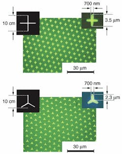
Because the microspheres have an enormous demagnification, the object-a single shape imaged repetitively by the microlens array-is macroscopic in scale (see figure). For example, creating images on the order of 4 æm in size with 6-æm microspheres requires that the object on the photomask be about 10 cm in size. Such a photomask is easily printed on a desktop printer in the form of an ordinary transparency.
Exposure takes from 0.5 to 4 min for a 0.5-æm-thick photoresist layer, depending on the type of ultraviolet light source and other variables. Aluminum structures a few microns in size, 50 nm thick, and with 700-nm linewidths were fabricated on zinc selenide.
The resonant frequency of the micropatterns was designed to be between 10 and 15 æm. The spectral transmittance of the structures was measured with a Fourier-transform infrared spectrometer. An array of crosses produced a resonance at 12.6 æm having a dip of 57% transmission, while tripoles resulted in a 12.3-æm resonance dipping to 63% transmission. Variations in microsphere size and other flaws broadened the width of the resonances.
Because millimeter-scale dimensional changes of the object result in 100-nm-scale changes in image dimensions, precise fine-tuning of microstructure shapes is possible; this, along with simple photomask fabrication, will allow researchers to test a wide variety of microstructure arrays quickly and inexpensively. Microlens arrays of 10 cm2 area and with periods approaching 1 æm will push spectral resonances to shorter wavelengths and array areas to commonly useful sizes; microlens arrays of high dimensional accuracy will be required to achieve large-area micropatterns with useful spectral qualities.
null
John Wallace
REFERENCE
1.Ming-Hsien Wu et al., Appl. Phys. Lett., (May 13, 2002).
TERAHERTZ IMAGING Fresnel lens yields three-dimensional measurements
While attempting to develop large, lightweight lenses for terahertz imaging, researchers at Rensselaer Polytechnic Institute (RPI; Troy, NY) believe that they may have stumbled across a new and potentially useful method of three-dimensional imaging.
Terahertz radiation occupies a large portion of the electromagnetic spectrum between the infrared and microwave bands from 0.1 to 10 THz. And although terahertz time-domain spectroscopy has been used for more than a decade to determine the optical properties of materials in the submillimeter wavelength regime, two-dimensional terahertz imaging has only been recently demonstrated, finding applications such as imaging semiconductors, leaf moisture content, flames, skin burn severity and skin cancer. Three-dimensional tomographic terahertz imaging methods are also under development (see Laser Focus World, May 2002, p. 133).
While focusing and collimating of terahertz radiation for imaging and time-domain spectroscopy has relied largely upon parabolic mirrors and silicon or polyethylene lenses, research on terahertz beams has been hampered by the difficulty of obtaining lenses for terahertz imaging with short focal lengths and large numerical apertures using silicon or polyethylene, according to X-C Zhang at RPI.1 In order to get around these difficulties, Zhang's research group was collaborating with another team at the University of Canterbury (Christchurch, New Zealand) to develop large-numerical-aperture terahertz-wave binary Fresnel lenses with short focal lengths by using modern planar microfabrication technology. The collaboration produced an unexpected result, however.
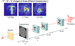
"We realized that the focal length of the Fresnel lens was linearly proportional to the wavelength of the beam," Zhang said. "Initially this was an annoyance that we wanted to get rid of. But then I thought, 'this could benefit us.' " Zhang wondered if the property could be used for tomographic imaging using the terahertz pulses that they were already working with, which were very short in the time domain but very broad in wavelength. So he tried it and it worked (see figure).
In the binary-lens tomography experiment, three 2 × 2-cm plastic sheets with 1 × 1-cm letter patterns were placed along the terahertz beam path. The three plastic sheets had 1-cm-height patterns of "T," "H," and "Z" placed 4, 6, and 15 cm from the beam, respectively. The object distance z' was fixed at 5.7 cm. The magnification factor (z'/z) for each letter was 1.43, 0.95, and 0.38, respectively, and the measured heights for the "T," "H," and "Z" images were 1.41, 0.95, and 0.39 cm, respectively, which agreed well with the calculated magnification factor.
Images of 2-D targets
The terahertz-wave Fresnel lens consisted of a 30-mm-diameter silicon binary element partitioned into 14 zones. The objects to be imaged consisted of three plastic sheets containing single- letter stencils. A temporal waveform at each pixel on the image plane was measured using a charge-coupled-device camera. A Fourier transformation of the temporal waveforms provided the terahertz field intensity distribution on the image plane at each frequency. The image of the terahertz field intensity at each frequency corresponded to a specific target distance from the Fresnel lens.
"We obtained images of 2 × 2-cm2 two-dimensional (2-D) targets with a z-distribution greater than 10 cm," Zhang said. "Our demonstration uses broadband terahertz radiation as the imaging beam, but the concept should also be applicable to a tunable narrowband imaging beam, as well as to other frequency ranges, including the visible."
While most spatial-imaging methods use a reflective time-of-flight method, the Fresnel lens method offers a transmissive position-sensing alternative, potentially useful for certain target-sensing applications. "But there is one thing that we have to make clear," Zhang said. "Because we use the imaging frequency to identify the location, we cannot take spectroscopy data to provide functional imaging in the way that we did before. This is the one drawback in using wavelength to label the distance z."
Despite the simplicity of the technique, Zhang said that his literature searches and discussions with colleagues at several institutions have not yet turned up previous work by others in frequency-dependent binary lens terahertz tomographic imaging. So he believes that he is breaking new ground. His next research objectives are to make the lenses larger, from 20 to 40 cm in diameter, and to image at distances ranging from 1 to 10 m at a scale that might be useful for imaging applications such as one might find in airport security. Going to such large sizes will probably require the use of a material other than silicon, and the RPI team has already begun the design process in polyethylene.
Hassaun A. Jones-Bey
REFERENCE
1.S. Wang et al., Opt. Lett. 27(13) 1183 (July 1, 2002).
PULSE MEASUREMENT Supercontinuum pulses get a case of the 'measles'
null
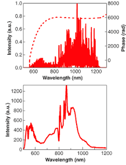
Since the introduction of microstructure fiber three years ago, researchers have been generating ultrabroadband white-light continua by propagating sub-nanojoule 800-nm pulses through this fiber.1 All experiments confirmed a broad, smooth, and remarkably stable spectrum. To fully characterize the continuum pulses, a group of scientists at Georgia Institute of Technology (Atlanta, GA) performed a cross- correlation frequency-resolved optical-gating (FROG) measurement of the spectrum and found a puzzling problem.
Measuring the intensity and phase of this continuum is inherently complicated. First, any multishot measurement requires that all the continuum pulses in the train be identical. Second, the nonlinear optical process used to make the measurement must have a massive phase-matching bandwidth exceeding that of the continuum. Third, while the precise time-bandwidth product (TBP) of the continuum was unknown, preliminary measurements indicated that it is very large (approximately 1000), making it the most complex ultrashort laser pulse ever generated. The most complex pulse ever measured previously had a TBP of about 10.
When Xun Gu, a graduate student at Georgia Tech, made these measurements, he found a substantial discrepancy between the FROG trace and the trace obtained by the FROG algorithm. The retrieved FROG trace, which is essentially a spectrogram showing the parabolic temporo-spectral profile of the continuum pulse, revealed a polka-dot pattern not contained in the measured trace.2 "My grad students called it the measles," said Rick Trebino, professor of physics at the Georgia Institute of Technology and founder of Swamp Optics (Lawrenceville, GA). Also, the FROG-retrieved spectrum was very complex, in stark contrast to all previous measurements of the continuum spectrum.
Normally when two measurements give different results, the cause of the discrepancy would be the more complex technique, which is the FROG measurement here. After Xu and the team identified every conceivable source of error, including phase-matching efficiency, camera response, and spectral resolution, the discrepancy remained (see Fig. 1).
Because a FROG trace is a two-dimensional joint time-frequency representation of a pulse, the two dimensions are simply two pictures of the same pulse. Missing information in one domain in principle can appear in the other domain, making such measurements quite reliable. In this case of continuum measurement, explains Trebino, "We then began to suspect the seemingly simple spectral measurements."
Highly structured spectrum
The spectral structure does not show in an independently measured spectrum or a FROG trace measured over many pulses, possibly because the structure is unstable and varies from shot to shot. Because a spectrum measurement or a multishot FROG procedure normally involves integrating as many as 1011 shots, the structure washes out, giving a smooth spectrum or FROG trace. However, the fine structure in the spectrum also takes other slowly varying forms in the time domain, leading FROG toward a qualitatively correct solution-a highly structured spectrum and a cubic spectral phase.
To confirm the theory, Xu performed single-shot spectral measurements of the microstructure-fiber continuum. The output pulse from a Ti:sapphire oscillator was amplified by an adjustable-repetition-rate regenerative amplifier to approximately 100 æJ per pulse, which was then attenuated to approximately 1 nJ for input into a microstructure fiber 152 cm long and 2 æm in diameter (see Fig. 2).
Single-shot spectra always exhibited extreme amounts of fine-scale structure, in agreement with FROG measurements; furthermore, the structure was unstable and shifted from shot to shot. The results indicated that smooth continuum spectra from even the most stable unamplified oscillator must involve averaging over many highly structured individual spectra.
Theoretical modeling of continuum generation in microstructure fiber also predicts fine structure in the spectrum. Simulations by Alex Gaeta at Cornell show that the features are very sensitive to pump input power.3 "People didn't believe it at first," said Trebino. "What was believed to be beautiful and stable ends up being ugly. But it may be quite useful because the spectral phase is more stable, and that's more important."
Valerie C. Coffey
REFERENCES
- J. K. Ranka, R. S. Windeler, and A. J. Stentz, Opt. Lett. 25, 25 (2000).
- Xun Gu, et al., Opt. Lett., accepted for publication (2002).
- A. Gaeta, Opt. Lett., accepted for publication (2002).
null
FREE-SPACE COMMUNICATIONS Laser TV transmission makes trains safer
null
Vector Technology (Abertillery, Wales) has won a contract to provide platform-to-train communications for the Kowloon-Canton Railway Corporation's West Rail extension in Hong Kong, using the company's optical laser-interface technology (OLI). The two-year contract has been issued through Siemens (Munich, Germany), the prime contractor.
Vector Technology installed its first OLI-based system, also in Hong Kong, in 1998, and since then the company has gained experience providing optical hardware for railways. The OLI is used to transmit real-time color closed-circuit television (CCTV) pictures from the platform to a moving train before, during and just after it stops at the station. The CCTV signal is superimposed on the light beam emitted from an infrared laser; a power of 30 to 40 mW from 808-nm-emitting diode lasers is used. The signal is carried up to 1500 m via a standard optical fiber. The signal from the fiber is routed to a projector mounted alongside the track. The output beam is shaped with holographic optics and then transmitted through free space to a receiver mounted on the train, where it is converted back to a video display.
The projected beam from the transmitter heads-which is tailored to ensure a "Class I" power level for safety-can provide a continuous signal over a 500-m distance. The train-borne receiver heads each consist of a two- element lens system-the first to collect light, and the second to maximize off-axis performance. Together with a photodiode, this configuration results in a horizontal acceptance angle greater than 12
The platform-to-train system can transmit two channels of broadcast-quality color video with a signal-to-noise performance of better than 40 dB at maximum range. The system can also be expanded to provide the driver with CCTV coverage from each of the carriages in the train. In this case, there is a free-space link from carriage to carriage. In addition, the system can be used to give the driver CCTV pictures of potential hazard points such as level crossings, road bridges, and busy intersections to a distance of up to several miles ahead, and can be used as a reciprocal train-to-platform communication system. Installation starts in November 2002, with the line scheduled to open in 2004.
Bridget Marx
IMAGE PROCESSING Software links microscopy images with quantitative biological data
null
Regardless of whether a picture, according to the well-worn clich is actually worth 1000 words, the fact is that modern science often wants both the pictures and the words. This is particularly true in the burgeoning discipline of genomics, in which a brief glimpse of even the most elementary processes can require at least 1000 pictures.
To help biological researchers make sense of this torrent of images and words, scientists at Lawrence Berkeley National Laboratory (LBNL; Berkeley, CA) have developed a World Wide Web-based computer program called BioSig that links microscopy images to quantitative data, performs sophisticated image and data analyses, and then serves up requested data on demand in user-friendly presentations.1 In addition to helping biologists understand various genomes, BioSig may also help biologists understand each other, according to Mary Helen Barcellos-Hoff, a life scientist at LBNL and co-principal investigator on the BioSig project.
"Cell biologists love a good microscope image," she said, "but a radiation biologist is likely to say, 'Well, that's pretty, but what does it mean?' Radiation biology is classically a quantitative field. It has been difficult to put new information gained from microscopy into quantitative form."
The other co-principal investigator on the project, computer scientist Bahram Parvin, described the problem from a complementary perspective. "How do you represent images so that such a representation reduces the data volume, and at the same time is information preserving?" he asked. "What quantifiable insights can you obtain from an image collection?"
Phenomics
Barcellos-Hoff and Parvin have taken on this challenge in the field of functional genomics that they have dubbed "phenomics," where scientists seek to understand the expression of genomes into countless variations of cell phenotypes. The task requires tracking the kinetics and quantities of multiple cellular proteins, as well as their cellular environments, and their morphological features in large populations. It also includes tracking the effects of thousands of antibodies and reagents that differentiate a cell's specific protein components.
In a typical experiment, researchers prepare tissue sections and stain them to localize a protein of interest for detection using fluorochromes that can be excited by stimulation of specific wavelengths of light. The web-based informatics system developed by Barcellos-Hoff and Parvin essentially transforms each such experiment into an accessible online library entry by archiving the experimentally obtained images and all of the scientific notebook annotations that go with those images for subsequent postprocessing and viewing (see figure).
The software uses three components to accomplish this. The first, a data-model component, gathers the experimental data and sample preparation variables along with the images and maps the data to the images. The second, a presentation manager, provides a map between the data model and the user interface and also displays biological functions in text and graphic forms. The third, a query manager, essentially uses Java objects to provide user-friendly data analyses in response to user queries.
Faced with the difficulty of segmenting specific cellular compartments in an image environment full of technical variability in sample preparation, nonuniform staining of samples, noisy images, and overlap of subcellular components, the researchers developed an automatic segmentation method to remove noise and outline each cell or nucleus. The method recognizes curved sections of the envelopes or membranes of nuclei and calculates individual "centroids" that enable adjacent objects to be distinguished even when they overlap. Further calculations precisely determine the location and magnitude of expressed proteins identified by specific antibodies.
Barcellos-Hoff and Parvin have successfully tested the program in an in vitro study of human breast cells and an in vivo study of mouse mammary cells. In the in vitro study, researchers were able to establish the pathways by which radiation and a protein modifier, acting separately and together, affect the formation of crucial structures in human breast cells. In the in vivo study, the software was used to quantify a link between an extracellular factor and intracellular response in mouse mammary glands.
The focus of the BioSig project is to enable researchers to save and access large amounts of quantitative information in images and to ultimately makes the images useful in ways never before practical. The system is also intended to constitute a hypothesis-generating data model with the potential for testing new ideas by querying experimental information in an existing database, as well as importing "legacy" data, which may have been gathered for a completely different purpose. More information can be found online at http://vision.lbl.gov/Projects/bioinformatic/index.htm.
Hassaun A. Jones-Bey
REFERENCE
1.B. Parvin et al., Computer 35(7) 11 (July 2002).
MATERIALS SCIENCE Spanish researchers question claim of 'perfect lens'
null
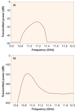
Experimental verification in early 2001 of a negative index of refraction has been countered by scientists who say the claims are questionable. An experimental "left-handed material" consisting of copper split-ring resonators was demonstrated by scientists at the University of California, San Diego (UCSD; La Jolla, CA), that exhibited a negative effective index of refraction at microwave frequencies (see Laser Focus World, February 2001, p. 38).1 An optical material with such a negative refractive index could amplify evanescent waves, thereby acting as a "perfect lens," a possibility proposed by John Pendry of Imperial College (London, England) two years ago.2 Such a material would have potential application to beam steering, bandpass filters, and lenses with subwavelength point-source focusing.
But Manuel Nieto-Vesperinas and Nicolas Garcia of the Instituto de Ciencia de Materiales (Madrid, Spain) point out that absorption losses dominate in the UCSD material, causing it to behave like a metal.3 Evanescent waves in an ideal left-handed material are amplified, the two researchers confirm, but their restoration would involve infinite energy, and absorption causes them to decay anyway.4
"The losses kill everything," says Nieto-Vesperinas. "We believe in the existence of negative-index media and negative refraction," he adds, "but in structures unlike those built so far."
Negative response
David Smith, professor of physics at UCSD stands by his results, saying that his experiment constructed a "metamaterial"-an artificially structured medium using split-ring resonators to produce an effective negative permeability, and wires to produce an effective negative-permittivity response.
"Garcia and Nieto- Vesperinas accept the derived effective medium form for the split-ring resonators," says Smith, "but make use of an alternate theory to arrive at the effective permittivity due to the wire medium. They conclude that the wire medium, rather than being characterized by a moderate negative permittivity, is, rather, characterized by a very large imaginary permittivity."
In the UCSD experiment, the wire medium was composed of lithographically deposited stripes, periodically positioned, measuring 30
The UCSD team claims that its measurements, simulations, and theory are self-consistent. "A preponderance of the data suggests the correct interpretation of materials is that they are characterized by negative indices of refraction," says Smith. "While finite conductivity and substrate losses may contribute to a significant imaginary part of the permittivity and permeability, the amount of losses in these materials is not sufficient to override the interpretation of negative index."
Garcia agrees that in theory, for thick wires, the left-handed material has low losses, but, he insists, the numbers show that in Smith's experiment, losses dominate. "The material is not left-handed," he says.
Other recent papers have also disagreed with the work by Pendry and UCSD for various reasons. Pendry has submitted several comments to Physics Review Letters defending his theory, and says he looks forward to the continuing exchange of ideas. Although the interpretations vary, most of the experts agree with Pendry that "the real challenge is the practical one of designing very low-loss negative-index mediums."
Valerie C. Coffey
REFERENCES
- R. A. Shelby et al., Science 292, 77 (2001).
- J. B. Pendry, Phys. Rev. Lett. 85, 3966 (2000).
- N. Garcia and M. Nieto-Vesperinas, Opt. Lett. 27, 885 (2002).
- N. Garcia and M. Nieto-Vesperinas, Phys. Rev. Lett. 88, 207403 (2002).
SEMICONDUCTOR EMITTERS Laser-deposition technique grows nitride LEDs easily
The interest in group-III nitride thin film devices grew considerably upon the development of gallium nitride (GaN)-based lasers in 1996. To generate layers for these devices, different epitaxial growth techniques are used, such as metalorganic chemical-vapor deposition (MOCVD), pulsed-laser deposition (PLD), and molecular-beam epitaxy (MBE). The goal is to achieve high-quality monocrystalline layers, requiring appropriate selection of target materials and careful control of the deposition parameters. At the Institute of Technical Physics of the German Aerospace Center (Stuttgart, Germany), researchers have developed a modified PLD technique that has several advantages over well-established techniques.1, 2
Standard deposition techniques have disadvantages. In PLD, compounds such as ceramics or pressed powder nitrides usually must be used as the targets. For MBE, ultrahigh-vacuum conditions are required. The handling of metalorganic precursors used in MOCVD requires considerable safety equipment. In the new, modified PLD technique, called laser-induced reactive epitaxy (LIRE), standard high-vacuum conditions are sufficient, while ordinary molecular nitrogen is used as process gas. As the targets, pure metals, alloys, or metals that contain the dopants in a premixture are used. The deposition parameters can be conveniently controlled by the laser pulse energy.
The researchers used an Nd:YAG laser emitting 8-ns pulses at a 1064-nm wavelength, 4-kHz repetition rate, and 1.7- to 2.2-mJ pulse energy for focusing onto molten metal targets, reaching a power density of 109 W/cm2 at the focal spot. An ablation plume was generated. The rotatable and heatable target holder could handle up to four different materials. Molecular nitrogen conducted into the chamber produced a pressure of 0.10 to 0.13 mbar. Atomic nitrogen was generated in the shock wave of the expanding metallic ablation plume.
Deposition is even
The yield could be monitored spectroscopically; hence, by balancing the nitrogen flow and the laser pulse energy density, the III/V ratio could be controlled. The substrates used were 1-in. sapphire in the (0001) orientation. Due to the comparatively high gas pressure (with respect to MBE), the atoms were efficiently thermalized and spread out, favoring a homogeneous deposition. In this way, indium aluminum gallium nitride (InAlGaN) films were grown and subsequently analyzed by different methods such as cathodoluminescence, scanning-electron microscopy, micro-Raman spectroscopy, and Hall measurements; film thicknesses were measured by ellipsometry.
To demonstrate a functioning optoelectronic component, a stack of different layers was deposited, starting with a base layer to invert the polarity of the following layers, followed by a buffer layer, n-type GaN, the active InGaN layer, and a p-type layer (see figure). The spectral emission of an InGaN light-emitting diode produced in this way peaked at about 500 nm.
The experiments show that LIRE has become an interesting alternative with respect to the existing methods. For a 10-W laser power, the deposition rates for LIRE are typically 1 æm/h-comparable to existing methods. Creating the lower-quality vacuum required for LIRE is easier, however, and the associated equipment less costly.
Uwe Brinkmann
REFERENCES
- T. Rupp, G. Henn, M. Gross, H. Schr?der, Appl. Phys. A 69, 799 (1999).
- T. Rupp, G. Henn, H. Schr?der, Appl. Surf. Sci. 186, 429 (2002).

