Semiconductor laser emits terahertz radiation
A quantum-cascade prototype laser demonstrated by Italian researchers at the Scuola Normale Superiore at NEST-INFM (Pisa, Italy) is the first semiconductor heterostructure source capable of emitting terahertz radiation.1 Conventional sources in this wavelength range, such as gas lasers, Auston switches, or photomixing, suffer from different shortcomings, preventing their widespread use. For example, sources based on oscillating charges generate only very low output powers, and the p-doped germanium laser is inherently limited to cryogenic temperatures. A terahertz device has many applications in medical imaging, astronomy, and process monitoring.
The terahertz region of the electromagnetic spectrum is characterized by a lack of compact, low-consumption, solid-state sources. So far, neither electronic devices nor semiconductor lasers emit in this intermediate region between visible/infrared and microwave/radio frequencies. Conventional semiconductor diode lasers, based on transitions between the conduction and valence band, are unlikely to ever reach into the far-infrared or terahertz region, due to both fundamental and technological problems. However, the quantum cascade (QC) laser is a promising candidate because the optical transition occurs within the conduction band between states originating from quantum confinement. Therefore, the bandgap of the constituent materials is irrelevant to QC operation and a mature material system like gallium arsenide/aluminum gallium arsenide (GaAs/AlGaAs) can be used.
Although research has extended the wavelength of QC lasers to longer wavelengths, the frequencies are still limited to more than 12 THz. "Our work was stimulated by the numerous applications of terahertz radiation, which all are just at birth owing to the lack of an appropriate source," says Ruedeger Kohler, principal investigator of the project at NEST-INFM.
A complement to x-rays
Because of the much lower photon energy, a terahertz QC laser could yield information complementary to conventional x-rays without harming biological tissue. Furthermore, terahertz wavelengths are sensitive to different types of tissue, such as nerves, blood vessels, fat, and sinews, which allows, for example, the detection of cavities and early states of skin cancer. Another interesting application is in security screening as clothing and plastics are completely transparent, while metals are opaque. Moreover, toxic gases and explosives have characteristic spectral fingerprints in the terahertz region. Finally, the available bandwidth of terahertz radiation is much higher than that of current radio-frequency and microwave wireless local-area networks, which would allow faster communication links.
The waveguide and the electronic structure of the active material were designed at NEST-INFM. The structure of the prototype was fabricated at the University of Cambridge (Cambridge, England) using molecular beam epitaxy (MBE). The synthesized structures were then sent back to NEST-INFM to be fabricated and characterized. The Politecnico (Turin, Italy) provided a Monte Carlo simulation of the electron dynamics and transport characteristics.
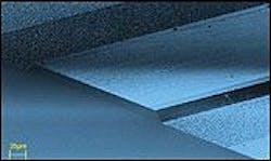
In the device, current is injected downward through a gold contact on top of the ridge, which measures 180 μm x 1.5 mm (see Fig. 1). The ridge comprises about 1500 vertical layers of GaAs and AlGaAs, making up 100 periods of the active heterostructure. Light propagates along the ridge, guided by a thin, high-doped GaAs layer underneath the 10.3-μm-thick stack of active regions.
Calculations help visualize the intensity profile of the emission (see Fig. 2). As the optical mode propagates across the laser ridge, the calculated intensity profile exits parallel to the laser facet. A thin, high-doped GaAs layer guides the optical mode at the bottom of the ridge, cutting a notch into the mode profile, and decays into the undoped substrate below that layer. The overlap of the mode with the stack of active regions (confinement factor) is approximately 50%; the laser has a vacuum wavelength of 67 μm and an epilayer thickness of 11 μm.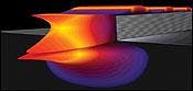
The prototype currently operates at temperatures up to 60 K. Most applications require a liquid-nitrogen temperature of 80 K. To reach this temperature hallmark, the NEST-INFM team is improving the design and device processing. A near-future goal is continuous-wave operation of the laser. These goals would render the device suitable for applications in which portability is not required, such as in medical imaging or security screening. Long-term goals, says Kohler, include operation at higher temperatures, accessible with Stirling or Peltier coolers, and room-temperature operation.
REFERENCE
1. Ruedeger Kohler et al., Nature 417, 156 (2002).
About the Author

Valerie Coffey-Rosich
Contributing Editor
Valerie Coffey-Rosich is a freelance science and technology writer and editor and a contributing editor for Laser Focus World; she previously served as an Associate Technical Editor (2000-2003) and a Senior Technical Editor (2007-2008) for Laser Focus World.
Valerie holds a BS in physics from the University of Nevada, Reno, and an MA in astronomy from Boston University. She specializes in editing and writing about optics, photonics, astronomy, and physics in academic, reference, and business-to-business publications. In addition to Laser Focus World, her work has appeared online and in print for clients such as the American Institute of Physics, American Heritage Dictionary, BioPhotonics, Encyclopedia Britannica, EuroPhotonics, the Optical Society of America, Photonics Focus, Photonics Spectra, Sky & Telescope, and many others. She is based in Palm Springs, California.