Color electroluminescent displays use nanocrystals
Most full-color displays in use today are still based on indirect generation of pixel colors: cathode-ray tubes need an electron beam for excitation of phosphors, while liquid-crystal displays and thin-film-transistor displays rely on white-light sources and optical filtering. Direct emission of the three required pixel colors—red, green, and blue—is simpler; hence, light-emitting diodes, organic light-emitting diodes, and plasma diodes are in the offing to replace the more-standard technologies. Another interesting alternative is under study at the University of Munich, where researchers have introduced electric-field-directed layer-by-layer assembly (EFDLA) of luminescent nanocrystals, which allows the preselection of emission color by particle size.1 Deposition is provided by the controlled precipitation of the particles (crystals) from a liquid onto an electrode, a technique that can be scaled to pixellated arrays.
The technique is based on layer-by-layer assembly of ultrathin films. Layer-by-layer methods result in films with better quality for optoelectronic applications than films fabricated with Langmuir-Blodgett and spin-coating techniques. Using lithographic approaches, lateral structuring with binary or ternary patterns of different self-assembled films has been successfully demonstrated using different chemical and physicochemical interactions for the binding of the various films to the substrate. The Munich group extended this technology to produce not only well-defined heterolayers in the direction perpendicular to the substrate, but also to create lateral patterns. Electrophoretic deposition could be performed on a lithographically generated conductive microstructure. This opened the door to addressing pixels electrically and exciting them to luminesce.
Conductive indium tin oxide glass was used as a dual-electrode structure, with the two electrodes fabricated by masking and etching. Negatively charged fluorescent cadmium telluride (CdTe) nanocrystals of well-defined size and a positively charged polyelectrolyte—poly(diallyl dimethyl ammonium chloride; PDDA)—were successively deposited from an aqueous solution on one of the electrodes by applying a voltage opposite to the polarity of the material to be deposited, favoring deposition. Performed by a robot, the entire growth process consists of a series of dipping and washing procedures in various aqueous solutions. The polarity of the second electrode was kept at an unfavorable equal polarity so that no deposition occurred. In such a way, a system of anioncation bilayers—that is, a CdTe/PDAA bilayer repeated N times to make a multibilayer—was generated (N ranging from 40 to 60). The multibilayer contained CdTe particles of about 2.5-nm diameter. A quartz crystal microbalance was used to calibrate the deposition thickness.
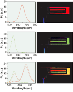
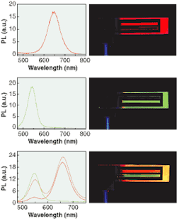
FIGURE 1. Electrode structures are created by electric-field-directed layer-by-layer assembly. Structures with U-shaped margins fluoresce in red or green (top and center) and in both colors (bottom), appearing as orange on the margin due to superposition. At left are the corresponding spectra. Red is obtained from the upper electrode (and from the margin, which accepts deposition as long as no repelling voltage is applied) alone; green from the bottom electrode alone; and, with both electrodes stimulated and emitting in their respective colors, orange from the margin (the combination of green and red).
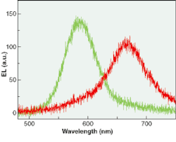
FIGURE 2. Electroluminescence spectra of red- and green-emitting pixels are slightly redshifted from their fluorescence spectra.
Two-color operation
In a different role, the second electrode could be coated with a similar multibilayer with a slightly different particle size (3.5-nm diameter). It is well known that, due to the quantum confinement effect, absorption and photoluminescence spectra can be tuned to longer wavelengths with increasing particle size. In this case, 2.5-nm particles yielded green emission, while 3.5-nm particles yielded red.
Results were obtained for three structures, each made of a U-shaped margin, to which no voltage was applied, and two inner electrodes with voltages oppositely controlled so that one of them is coated by CdTe nanocrystals (see Fig. 1). Electroluminescent pixels were then prepared by depositing a thin aluminum electrode of 140-nm thickness. Their electroluminescence spectra showed a small redshift with respect to fluorescence (see Fig. 2).
The experiments show that color-specific creation of pixels based on the deposition of layers containing particles of different sizes is feasible by combining electrophoretic deposition and layer-by-layer assembly. The same electrodes used to control the deposition process can then be used to address active pixels. This combination of layer-by-layer assembly and electrophoresis is not restricted to CdTe nanocrystals. Water-soluble core/shell nanocrystals as well as water-soluble conjugated polymers can be used in EFDLA; moreover, the technique is not restricted to the creation of pixel arrays for displays, but could also be used for the realization of bioassays.
REFERENCE
- M. Gao et al., Langmuir 18, 4098 (2002).


