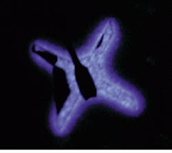
Researchers at the Institut für Halbleitertechnik at the Technical University of Aachen (RWTH; Aachen, Germany) have developed a gallium nitride (GaN) based blue (443-nm) light-emitting diode (LED; see figure). Team member Bernd Schineller says that “no lifetime measurements were carried out” on the room-temperature-emission LED, “but at this time we don’t see any problems. The device operation is stable for several hours.” The device is the result of joint research with Aixtron (Aachen, Germany), a company spinoff of RWTH, investigating semiconductor structural growth, processing, measurement, and analysis and material performance. The work was funded by the company.
One area of investigation is growth and activation of magnesium-doped group-III nitrides. The work includes experiments on proprietary postgrowth annealing processes, both within the reactor and in an external rapid thermal-annealing furnace. Structures involved are magnesium-doped single layers; electrical properties, photoluminescence measurement, and x-ray imaging are used for assessment.
Another approach, resulting in the reported blue LED, looks at the effects of growth and postgrowth treatments on characteristics such as efficiency, intensity current, series resistance, spectral output, and turn-on and operating voltages of emitter structures. The characteristics, in turn, can be used to monitor the growth processes. A structure of sapphire/GaN buffer/AlGaN:Si/GaN:n.i.d. (not intentionally doped)/AlGaN:Mg emitted at 443 nm, with wavelength dependent on the doping concentration. During growth of the n.i.d. layer, the doping precursors are switched off. The active GaN:n.i.d. layer is 50 nm thick, while the other layers are on the order of 1 µm. Schineller notes, “We see this simple device structure primarily as a tool for growth and annealing optimization. No changes in the structure are planned at this point.”
Device characteristics include an emission threshold current of 200 µA and operating current of 1 mA at 3.61 V and 20 mA at 7 V. Light intensity was nearly linear with current up to 5 mA. Applications include optimization not only of LEDs but also of lasers and high-power field-effect transistors and the metal-organic vapor-phase epitaxy production process.
The LED material was fabricated using a research version of an Aixtron reactor. A pure laminar (turbulence-free) horizontal flow in the reactor allowed precise control of material composition and “ultrasharp” interfaces on a monolayer scale. A proprietary “purged window” technique allowed process monitoring and wafer mapping during fabrication.
The institute studies correlations between materials and their methods of production, properties, and devices made from them.
About the Author
Rick DeMeis
Associate Editor, Technology
Rick DeMeis was Associate Editor, Technology for Laser Focus World from March 1995 through March 1997.
