Low-temperature process enables monolithic devices
A prototype optoelectronic-integrated-circuit (OEIC) foundry for nine university research groups is being used to test a process for fabricating OEICs—monolithic circuits that integrate both electronic and optical devices. The goal of the project is to provide each research group with six working chips made to their design. “If all goes well, the chips should be done by mid-February,” says Joseph Ahadian at the Massachusetts Institute of Technology Research Laboratory for Electronics (MIT; Cambridge, MA).
The lack of a practical method for making chips that are a combination of very-large-scale integrated (VLSI) electronics with light emitters and detectors is currently a major barrier to commercial OEIC fabrication. Electronic chips are typically made with silicon, which is incompatible with the materials from which lasers and light-emitting diodes (LEDs) are made.
Ahadian and others working with Clifton Fonstad and Leslie Kolodziejski at MIT are bypassing the materials problem by using gallium arsenide (GaAs) for both the VLSI electronics and the light emitters. The MIT group, along with P. T. Vaidyanathan and Sheila Prasad at Northeastern University (Boston, MA) have developed a process for fabricating optoelectronic devices on wafers that have VLSI electronics already on them. This epitaxy-on-electronics technique is based on established manufacturing methods. The researchers described their work last November at the annual meeting of the Lasers and Electro-Optics Society (Boston, MA).
Low temperature enables growth
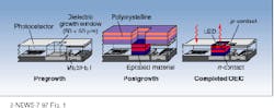
The GaAs wafers are grown with areas reserved for LEDs. A commercial foundry partially etches the interconnect dielectric stack in these regions, forming 50 50-µm windows for the LEDs. In fact, the windows can be made any size anywhere on the chip, says Ahadian. The MIT group finishes the etch before growing device heterostructures in the reserved areas with gas-source molecular-beam epitaxy (MBE).
The production of a high-quality GaAs starting surface is one of the innovations of the process. Conventional MBE begins by raising the substrate temperature to 580°C to desorb the GaAs native oxide before growth. The chips in this project are already metallized and cannot, therefore, withstand such high temperatures. Because the process must be kept below 475°C, atomic hydrogen is used to remove the oxide.
Using gas-source MBE, the LEDs are grown until nearly level with the original wafer surface (see Fig. 1). Because aluminum gallium arsenide (AlGaAs) requires growth temperatures higher than the 475°C limit, indium gallium arsenide phosphide (InGaAsP) is used for the emitter. After growth, the devices are connected to the electronics through top-side contacts. Light-emitting diodes based on GaAs/InGaAsP and emitting around 870 nm have been grown on the chips with useful output powers and external quantum efficiencies exceeding 1%. Preliminary testing shows that the GaAs electronics maintains its subnanosecond speeds following the epitaxy-on-electronics process.
“We chose LEDs because we thought they would be easier to fabricate than lasers,” says Ahadian, “but it makes no difference to the integration process.” The researchers’ next step will be to demonstrate chips with surface-emitting lasers, either vertical-cavity surface-emitting lasers (VCSELs) or in-plane surface-emitting lasers. Although, these latter devices require a sophisticated etching process to produce upturned mirrors, they have advantages with regard to thermal crosstalk.
Nonetheless, VCSELs dissipate much lower power, which allows for integration of thousands of emitters on a single chip. While still an immature technology, current state-of-the-art VCSELs will make a welcome replacement for the LEDs now being integrated. Ahadian hopes to have integrated VCSELs within a year. But future work will require an advanced VCSEL design with reduced series resistance.
Optochip project tests designs
Meanwhile, the researchers are making the LED-on-VLSI technology available to nine optical-interconnect systems research groups at seven US universities—California Institute of Technology, University of Southern California, West Point, George Mason University, University of Washington, Texas Christian University, and Colorado State University—and McGill University in Canada. Eight designs for 2 2-mm OEICs have been accepted, ranging in complexity from simple emitter/detector arrays to complex, computer-synthesized circuits. The eight designs were compiled into a larger die that will be cut apart following the integration process.
Optical interconnections are promising techniques for next-generation high-speed computing and telecommunications systems, but development has been hampered by the lack of a foundry for such devices. For experimental work, a silicon substrate has been used—epitaxial lift-off methods enable thin films of emitters grown on GaAs to be attached—but the commercial viability of this hybrid technique is unproven. Until recently, no commercial source could provide VLSI electronics based on GaAs, so researchers who wanted to build on a commercial basis were stuck with hybrid designs.
Increasing interest in high-speed circuitry has made GaAs-based circuits more pervasive because they operate at higher speeds than do silicon-based devices, and they dissipate much less power. The GaAs chips used by the MIT researchers are commercially fabricated by Vitesse Semiconductor Corp. (Camarillo, CA). Vitesse’s VLSI GaAs foundry and the robust epitaxy-on-electronics process developed at MIT have advanced the feasibility of monolithic OEICs, and the Optochip Project provides optical interconnect researchers with tools for testing their designs.