Display technologies continue to evolve that could someday replace bulky cathode-ray tubes (CRTs). At the Society for Information Display (SID) May `97 conference in Boston, Philips Research Laboratories (Eindhoven, Netherlands) demonstrated a new thin CRT device, while Canon Research Center (Kanagawa, Japan) demonstrated a new way of making field-emission displays (FEDs). But, even though new display technologies show technical promise, their commercialization is far from assured. Even as Philips engineers showed how well their thin CRT works, the company had quietly pulled the plug on the project (see "Market tough for new display technologies," p. 123). Despite the perils, many companies still pursue development of technologies for the $38 billion-a-year market for flat-panel display and CRTs. Plasma displays, long a dream for hang-on-the-wall television, are positioned to have a significant impact. Forty-inch (and soon 54-in.) displays will become commercially available from several sources (see Laser Focus World, July 1997, p. 34).
Field-emission displays, another contender, are still trying to find their commercial footing. While many teams are working on FEDs, so far only two companies, PixTech (Rousset, France) and Futaba (Chiba, Japan), have developed commercial products. These displays are still black and white and less than about 6 in. in diagonal but should move to color by the end of the year.
New approach to FEDs
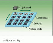
The surface-conduction-electron (SCE) display from Canon represents a new planar FED architecture that uses simple printing techniques and achieves high efficiency—as much as 10 lm/W.1 Most FEDs under commercial development use the microtip structure that comprises tiny conical electron emitters. To improve efficiency, the emitters are made as small as possible, usually submicron size. Thousands of them are then used for each pixel.
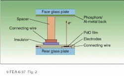
In the planar SCE process, electrons are emitted from a microfissure in a palladium oxide (PdO) film. The microfissure, which is perhaps only angstroms wide, emits electrons in an oval pattern, much like from a diode laser. Because only one microfissure pattern is used per pixel, there is not a very good match between the emission pattern and the square pixel shape. Consequently, SCE devices may be best suited for multimedia or TV applications, in which the pixels can be larger and more spread out.The connecting wires are formed with thick-film screen printing to produce a low-resistance addressable matrix (see Fig. 2). Spacers separate the anode faceplate, which contains standard P-22 R/G/B phosphors and is maintained at 15 kV.
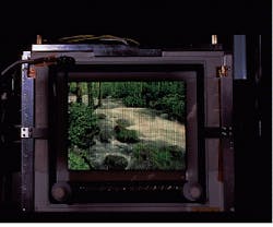
So far, Canon has shown a 10-in., 240 × 240 color display that is only 9.6 mm thick. With a white luminance of 690 cd/m2, contrast in excess of 1000:1, and a good color palette, the device has shown impressive video imagery (see photo, p. 121). Efficiency is so good that the company estimates a 40-in. device would consume only 53 W, less than one-forth the power used by plasma displays.
Perhaps the most important aspect is the simple manufacturing processes used to make this display. Not only can standard printing techniques be used, but they can be realized in air rather than vacuum. These processes allow the use of much less-expensive equipment and reduce consumption of materials—both significant cost factors.
Hopping electrons
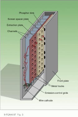
Philips has developed a cathode-ray panel (CRP) that uses a mechanism called "controlled (`hopping`) electron transport" through insulating structures.2,3 In papers presented at SID `97, the company described a 17-in. prototype and life-cycle tests underway on a 5-in. device.Electrons are generated by a single thermionic-wire cathode with the current for each channel (column) controlled by a pair of gate electrodes (see Fig. 3). (Many channels are needed to produce a full two-dimensional display.) These electrons are then drawn to the glass plate that forms the back surface of the device. Here, using a newly discovered phenomenon, electrons "hop" up the channel, creating a sea of electrons that are confined near the insulating surface of the back glass plate (see "How hopping electron transport works," p. 124).
A row is addressed by applying a voltage pulse (approximately 200 V) to the horizontal electrodes on the extraction plate. This pulse draws electrons from the back surface through the holes in the extraction plate to impinge upon the constriction plate, which is designed to help equalize the diverse energies of the extracted electrons.
Next, the selection plate is used to divert electrons through one of several apertures by applying another voltage pulse. Figure 3 shows two apertures, but for the prototype exhibited at SID `97, three apertures in a red-green-blue triad configuration were used. Exiting electrons pass between screen spacers to finally impinge upon either a red, green, or blue phosphor. These phosphors are deposited on yet another plate, which is maintained at about 4.5 kV.
Moreover, additional selection plates can be stacked to obtain a multiplexing capability, allowing a substantial reduction in the number of connections to the display. Reduction by a factor of 96 has been achieved on some devices.
The performance of the Philips device appears to be very close to CRT quality. For example, the color palette and viewing angles (about 180°) are similar to CRTs. Luminance (500 cd/m2 peak) and contrast (60:1 in 100-lux ambient light) are favorable for a prototype. The company claims it also has addressed manufacturing issues.
But even as these technical achievements were being described, management had decided not to fund further development. G. E. Thomas, a research director at Philips Research Laboratories, said, "The investments needed to bring this technology into the production phase are so high that it is very unlikely that another company would join in."
Despite the early exit of Philips, there may still be residual value in its achievement and demonstration of a new form of electron transport. Meanwhile the Canon development has shaken u¥the FED landscape, though it has yet to prove that the technology can be brought into full production. Nonetheless, electron-emission displays remain a technology to watch.
REFERENCES
1. E. Yamaguchi et al., Proc. SID `97 Vol. XXVIII, 52 (1997).
2. G. G. P. van Gorkom et al., Applied Surf. Science 111, 276 (1997).
3. G. G. P. van Gorkom et al., Proc. SID `97 Vol. XXVIII, 235 (1997).
Market tough for new display technologies
Many display technologies are developed every year, but few become commercial successes. Not only must the display performance be acceptable for the intended market, but it must withstand manufacturing and marketing considerations.
David Mentley, a display analyst at Stanford Resources (San Jose, CA), notes that "display technologies with only one company as the major supporter often fail in the marketplace. It doesn`t pay to develop the equipment and materials infrastructure to support single-company technologies."
Buyers of displays also like to have second sources. Philips Research Laboratories` decision to stop development of its thin CRT was driven by its inability to convince potential manufacturing partners to support commercialization of the cathode-ray-panel device, despite the fact that the display`s performance was quite good and many manufacturing issues had been addressed. While the company did not say exactly why potential partners balked, some observers speculated that competition with plasma displays may have played a big part. Both technologies were expected to compete for large-diagonal-display applications such as hang-on-the-wall TVs. Several large Japanese companies are now ramping up production of these displays, and Philips itself plans a plasma display product.
Philips is but the latest in a string of failed ventures. Matsushita tried to introduce a thin-CRT technology several years ago called FlatVision but reportedly had to withdraw the technology because of problems with uniformity and an inability to scale to larger display sizes.
Canon also has a poor track record in this area. Its efforts to commercialize ferroelectric displays never materialized, despite much effort and publicity. Successful commercialization of FEDs by Canon and other developers is an uphill battle, the outcome of which is still to be determined.
How hopping electron transport works
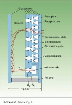
The cathode-ray panel developed by Philips Research Laboratories (Eindhoven, Netherlands) relies on an interesting new electron-transport mechanism that is essentially an electron-scattering phenomenon configured to allow its use in a display device.Early experiments with a simple insulating glass tube showed the potential. A wire cathode was placed at one end and used to inject electrons into the tube. A "transport voltage" was then applied between the entrance and exit of the glass tube. Above a threshold voltage, electrons suddenly reached the anode at the far end of the tube, producing a current.
But electrons are not in free flight down the center of the tube. Instead, they are interacting with the walls, producing secondary electrons that scatter in many directions. The visible luminescence of the glass tube verifies this effect.
As the transport voltage is in creased the electrons are confined closer to the glass surface, minimizing backscatter and producing mostly forward-scattered secondary electrons. Eventually, a self-regulating, steady-state situation results where one secondary electron is generated for each interaction with the wall. Such a situation is important because it allows the creation of a uniformly illuminated display. Deposition of a magnesium oxide layer enhances this process and lowers the threshold voltage.
Philips researchers adapted this effect with a new geometry suitable for a display device (see figure). The glass tube corresponds to the channel on the left side of the structure. The electron source has been moved from the tube end to enter from the side of the channel. The anode voltage is moved from the tube exit and established on the back of the extraction plate with a series of stripe electrodes. A linearly increasing dc voltage is applied to these extraction electrodes, establishing the gradient needed to produce the electron hopping mechanism indicated in the figure. With a 1.2 × 2.4-mm channel, a field of 80 V/cm is needed for good transport.
About the Author
Chris Chinnock
Chris Chinnock is president and owner of Insight Media in Norwalk, CT. He is a 30-year display industry veteran with experiences in displays, broadcast, cinema, ProAV, and consumer electronics.
