At Iowa State University (Ames, IA), researchers have demonstrated a simple method for designing single-photonic-crystal devices with waveguides efficiently connected in three spatial directions. Though initial experiments have been performed in the microwave region for ease of fabrication, the work is based on theoretical studies that, the researchers say, allow simple extension to optical wavelengths. In addition, they have shown that it is possible to construct a low-loss, easily aligned port for coupling light from fibers into these networks. All of these guides are built by simply removing (or not depositing) sections of the photonic-crystal rod structure.
Because the feature sizes in photonic crystals are in the micron-to-submicron size range, the obvious way to construct them is to use surface-microfabrication (layer-by-layer) techniques. An easy way to create the 3-D periodic structures required is to have alternating rods of high-refractive-index material in the x and y directions. Where they meet, perpendicular z-direction rods are built up, completing the structure. But avoiding the need for explicitly deposited z-direction features is a major advantage because such features are difficult to deposit and, generally, limited in height. If very large numbers of surface layers can be deposited, tight confinement in all directions is possible.
The Iowa State team demonstrated that this simple photonic-crystal structure and fabrication technique has another advantage: it is both conceptually and practically easy to create three-dimensional waveguides.1 The simplest approach is to leave out an entire horizontal rod in the direction of travel, or the sections of these rod that combine to create the vertical waveguide portions.
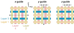
Through their simulations they discovered, however, that a slight modification of this technique produces more-efficient transitions between the guides. Instead of manipulating the y and z rods specifically, they omit sections from the x (or x and y) direction respectively (see Fig. 1). This technique allows guiding in both horizontal directions within the same layer—a far more efficient technique than trying to couple between waveguides created on adjacent layers. The researchers obtained losses as low as 0.5 dB for this type of bend.
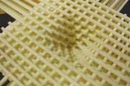
Unfortunately, the approach did not completely solve the problem in the vertical direction, in that part of the design bandwidth was not transmitted efficiently. In response, the team developed another approach known as a horn, which is essentially a pyramid structure cut out of the photonic crystal (see Fig. 2). In the first of two horn-based solutions to this problem, the researchers placed two horns back to back inside the crystal structure with the points of each touching a horizontal waveguide, allowing efficient coupling between layers. In this case, the coupling amplitude is at least as good as those of the narrow-channel bends and has the advantage of wider bandwidth.In the other approach, the point of the pyramid is coupled to a horizontal waveguide inside the crystal structure, and the base of the pyramid to the surface of the device, providing an efficient way of coupling in light from a fiber. Not only is the structure essentially self-aligning, but slight variations in the input angle do not have any serious effect on coupling efficiency, which can almost reach 100% for the design frequency. Researchers say that these two uses should considerably simplify the coupling of photonic-crystal devices, both with each other and with external components.
REFERENCES
- Curtis Sell et al., Appl. Phys. Lett. 84(23) (June 7, 2004).
- Curtis Sell et al., Appl. Phys. Lett. 85(5) (Aug. 2, 2004).
About the Author
Sunny Bains
Contributing Editor
Sunny Bains is a contributing editor for Laser Focus World and a technical journalist based in London, England.

