Researchers at Riken (Wako, Japan) have demonstrated a new way of making masks for optical lithography that is not constrained by the diffraction limit.1 The technique uses visible wavelengths and operates in the near-field, but does not rely on large optics. Also, unlike interferometry-based methods that only produce grating structures, researchers say they believe the surface-plasmon interference nanolithography technique should eventually be able to generate arbitrary sub-100-nm features. Success in this area will depend on the development of the right mathematical tools; the team is now collaborating with two companies to develop this side of the technology.
Three approaches have dominated the effort to turn microlithography into nanolithography. The most obvious is the development of sources with very short wavelengths (like extreme-UV and x-ray) and materials that can be used with them. Another approach is to allow interference with longer-wavelength sources; the resulting patterns have a much higher resolution than the diffraction-limited spot of the same wavelength. The main problem here is that such far-field diffraction patterns are not easy to control. More recently, there has been an interest in reducing the effective wavelength of light by having it travel inside a high-index medium and totally internally reflect. In this case, the near-field evanescent wave can be used to couple the high-resolution pattern into the photosensitive medium. Unfortunately, the density and curvature of the lenses required restricts the size of the pattern that can be imparted onto a flat substrate.
The new technique is, in a sense, a combination of all three of these techniques. It is based on the surface-plasmon polariton (SPP)—a wave of electronic oscillations that propagate along a metal surface when excited by incoming photons. If the metal is sufficiently thin, the oscillation goes all the way through and the resulting electromagnetic field creates light on the back side of the film. This photon/electron/photon interaction is useful for three reasons: the wavelength of an electron is much shorter than that of a visible photon, interference among SPPs allows the possibility of even smaller features, and these features can be coupled out as light in the near-field without a lens.
Choosing the right patterns
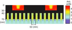
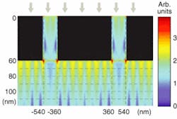
Key to controlling this process is the metal surface itself. Originally it was thought that the high transmission of light through metal films relied on holes patterned through them, but the team at Riken's Frontier Research System has shown that corrugation in the film can be used instead; perforations are not necessary. The trick is choosing the right combination of metallic input and output patterns in order to get the field distribution required. On the source side, periodic corrugations are used to collect energy, coupling it into SPPs as efficiently as possible. On the output side, engineered interference between SPPs using isolated metal features (produced using electron-beam lithography) can produce an arbitrary pattern in the high-resolution optical output.In one experiment using holes rather than corrugations, 100-nm-pitch gratings with 50-nm features were produced with a 12-s exposure at 436 nm. Simulation using finite-difference time-domain modeling suggests that 25-nm feature sizes should be possible using nonperforated geometry (see Fig. 1). The team has also shown how the features produced are dependent on interference (see Fig. 2). Even with holes separated by much more than a wavelength, feature sizes of 100 nm could be achieved. The researchers are now working to build mathematical tools that will allow them to work backward from an arbitrary near-field emission pattern to the thickness of the metal film used and the corrugations required on the input and output surfaces.
REFERENCE:
- X. Luo and T. Ishihara, Appl. Phys. Lett 84, 23 (2004).
About the Author
Sunny Bains
Contributing Editor
Sunny Bains is a contributing editor for Laser Focus World and a technical journalist based in London, England.

