Newsbreaks
Proton beam writes erbium-doped waveguide amplifiers
Along with sol-gel, femtosecond-laser-pulse, and other established techniques for fabricating erbium-doped waveguide amplifiers, now add proton-beam writing. Researchers at the University of Hong Kong (Kowloon, Hong Kong) and the National University of Singapore are writing buried-channel active waveguides in Er3+-Yb3+ codoped phosphate glasses using a focused beam of 2-MeV protons. Until now, the technique was used only to make passive waveguides.
At a dose of 1014 to 1015 ions/cm2 and a focal-spot size of 1 µm, the beam is moved through the glass and modifies the refractive index of the glass to create a waveguide 38 µm below the surface. After annealing, the approximately 8-µm-wide channels have an average propagation loss of 0.8 dB/cm. The amplified-spontaneous-emission spectrum of the glass in the waveguide is similar to that of bulk glass, indicating that the fabrication process does not affect the spectroscopic properties of the glass. When pumped with 100 mW of light at a 975-nm wavelength, the waveguides reach a maximum net gain of about 1.72 dB/cm at a wavelength of 1.534 µm and a full width at half maximum of 45 nm. Contact Edwin Pun at [email protected].
For field-emitter displays, closed-tip carbon nanotubes look better
Field-emitter displays (FEDs), in which electrons leaking from arrays of microscopic tips in a vacuum excite phosphors, were once touted as the next-generation replacement for liquid-crystal displays. Problems with the photolithographic fabrication of the tips, however, scuttled the technology for most purposes. But FED technology may be reborn, thanks to arrays of carbon nanotubes (CNTs) used as a replacement for the old-style tips. Not only are CNTs easier to make, but their much-sharper ends produce more electrons. Research is ongoing to find the best CNT characteristics for the job.
For example, scientists at Seoul National University have compared field emissions between arrays of CNTs with closed hemispherical ends and open ends and determined that closed is better. Using an aluminum plate with hexagonally arranged micropores as a template, arrays of both sorts of CNTs were grown with 110-nm tube spacings and heights varying from 50 to 160 nm. The field-enhancement factor peaked for both types of CNTs at a 110-nm tube height; however, the closed-end CNTs were three times more efficient at producing electrons for all tube heights. Contact Jung Sang Suh at [email protected].
Multiwavelength laser source scales easily
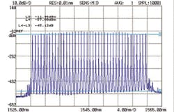
A multiwavelength semiconductor-laser source developed by engineers at Peleton Photonic Systems (Ottawa, Ontario, Canada) has properties such as small size and high scalability that show promise for use in dense wavelength-division multiplexing (DWDM). While current multiwavelength sources require a distributed-feedback (DFB) laser for every channel, the Peleton device contains just two single-frequency lasers in all and nonlinear fiberoptics that create the remainder of the channels.
Two conventional DFB sources with slightly differing wavelengths supply the input light. The nonlinear portion of the device consists of a spool of fiber within which four-wave mixing and other effects compress beat-frequency pulses to produce harmonics, resulting in channels that have a spacing set by the beat frequency. The channel spacing can be set arbitrarily. The entire package is slightly larger than a notebook computer. Scaling the device from, for example, 40 to 80 channels does not increase the number of components, and thus the proportional increase in cost is small. An optical post-processor flattens or otherwise modifies the spectrum. In addition to DWDM, Peleton engineers are aiming for applications in sensing. The device is being sampled to customers. Contact Robert Taylor at [email protected].
Waveguide allows higher photon energies from argon ions
By using a waveguide geometry to limit plasma-induced laser-beam defocusing, researchers at JILA, University of Colorado, and the National Institute of Standards and Technology (Boulder, CO) have generated high-order harmonics at extreme-ultraviolet (EUV) and soft x-ray wavelengths from ionized argon at energies 150 eV higher than any photons previously generated using 800-nm laser stimulation. Frequency upconversion in a gas of a near-IR femtosecond laser beam provides a tabletop-scale method under development by Colorado physicists to generate spatially coherent EUV light for applications that include EUV lithography, nanometer-scale imaging for biological and surface science applications, and ultrafast spectroscopy (see Laser Focus World, December 2004, p. 40).
An extreme nonlinear interaction between laser light and gas atoms produces the high-order harmonics in a coherent low-divergence beam; noble-gas atoms are preferred because of the relatively high energy photons they release. One major limit on the efficiency of the process to date, however, has been defocusing of the laser beam by the plasma that is generated in the ionizing interaction between the laser and the gas. The Colorado researchers used a hollow glass fiber filled with low-pressure gas to reduce the defocusing effect, allowing them to observe coherent emission from further ionization of argon ions up to 250 eV, as opposed to the previously observed maximum of 100 eV for argon using the same-wavelength driving laser. Contact Henry Kapteyn at [email protected].
Low-index photonic-crystal waveguides yield low-loss, single-mode transmission
Researchers at the Friedrich-Schiller University (Jena, Germany) have obtained low losses on the order of 1.7 dB/mm and quasi-single-mode propagation in a straight, low-index-contrast, photonic-crystal waveguide fabricated using niobium pentoxide glass sandwiched between silica films. Cross-sectional waveguide dimensions were on the order of 5 × 0.5 µm. Losses as low as 3 dB were achieved for a 60° bend in a similar waveguide. The structure consisted of a niobium pentoxide waveguide film (n of 2.17) within a cladding and buffer layer both made of silica (n of 1.43). The hole lattices consisted of 370-nm holes at a 595-nm pitch with nine rows omitted for the straight waveguide channel, and of 260-nm holes at a 595-nm pitch with five rows omitted for the bent waveguide channel. The researchers were also able to couple light efficiently into the bent waveguide using ridge-waveguide tapers. Contact Markus Augustin at [email protected].
'Funryu' allows 808-nm laser-diode bar to reach 255-W output
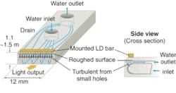
Researchers at Hamamatsu Photonics (Shizuoka, Japan) and Osaka University (Osaka, Japan) have developed a new type of heat sink a mere 1.1 mm thick that has allowed them to push the continuous-wave (CW) output power of an 808-nm-emitting laser-diode (LD) bar to new highs. The heat sink is called a "funryu," after the Japanese word for fountain, and is much simpler than the microchannel heat sink commonly used for LD bars.
Within the copper heat sink, cool water removes heat by turbulent flow through small holes that strikes a thin impingement plate beneath the LD bar. The impingement plate has a roughened inner surface to enhance heat transfer. A 1-cm LD bar with a 67% fill factor (70 laser diodes) was mounted to the funryu; the heat sink's 0.25°C/W thermal resistance allowed the LD bar to reach a maximum CW output of 255 W for a short time, and 167 W at the LD bar's maximum efficiency of 49.1%. The researchers expect the funryu to allow extended (several thousand hours) operation of an 808-nm-emitting LD bar at 80 W and 50% efficiency. Contact Hirofumi Miyajima at [email protected].
Gallium nitride–based LED may emit white light intrinsically
Two predominant ways to get white light from LEDs now exist. In one, a blue or UV-emitting LED is combined with a phosphor to produce an approximation of the white-light spectrum. In the other, the light from separate blue-, green-, and red-emitting LED chips are mingled to create white. Researchers at North Carolina State University (Raleigh, NC) and the U.S. Army Research Office (Research Triangle Park, NC) have developed a third approach, at least in theory.
Indium gallium nitride/gallium nitride (InGaN/GaN) LEDs can emit blue or green strongly, and red only weakly, with very poor efficiency. This occurs because a large internal field keeps the wave functions of holes and electrons apart; the effect results from a lattice mismatch between the well and the GaN quantum barrier. The researchers propose adding aluminum (Al) to the structure, replacing the GaN barrier with AlInGaAn and tailoring lattice mismatch. Simulations show that, with proper design, a single LED with three structures can produce blue, green, and red light of similar intensity and good efficiency. The researchers would like to fabricate such a device; one possible source of funding is the U.S. Department of Energy program on solid-state white-light sources, when it materializes. Contact Ki Wook Kim at [email protected].
Solar cell, heal thyself
If made practical, amorphous and polycrystalline sheet solar cells could end up perched atop many a commercial or residential roof. But the devices, which can range up to a square meter in size, suffer from reduced efficiency caused by micron-scale nonuniformities in grain size and chemical composition. Scientists at the University of Toledo (Toledo, OH) have developed a technique in which a thin-film semiconductor structure, when immersed in an electrolyte and exposed to light, modifies itself to compensate for the nonuniformities.
In one example, a cadmium telluride/cadmium sulphide (CdTe/CdS) photovoltaic device contains a 0.15-µm-thick layer of CdS and a 3.5- to 4-µm-thick layer of CdTe on glass. The electrolyte consists of sodium chloride, aniline, and p-toluenesulfonic acid in deionized water. When the electrolyte is applied to one side of the structure and tungsten-halogen lamp light to the other, changes occur that the researchers posit are the elimination of weak microdiodes and the depositing of a protective layer. The process improved the efficiency of CdTe/CdS cells from 1%–3% to 11%–12%. Contact Yann Roussillon at [email protected].
Stimulated Raman emission and wavelength conversion observed in silicon
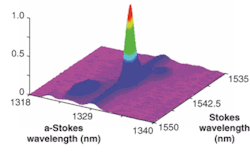
Building upon a previous demonstration of spontaneous Raman light emission from silicon waveguides (see Laser Focus World, April 2003, p. 19), researchers at the University of California-Los Angeles, in an effort supported by DARPA (the Defense Advanced Research Projects Agency), have demonstrated optical gain using stimulated Raman emission as well as wavelength conversion in silicon. They observed amplification of the Stokes signal up to 0.25 dB at 1542.3 nm using a 1427-nm pump laser at a 1.6-W continuous-wave power in a silicon-on-insulator waveguide. Coherent anti-Stokes Raman scattering (CARS), a combination of Raman and four-wave mixing, enabled the wavelength conversion from 1542.3 nm to 1328.8 nm using the same pump laser.
The CARS method couples two pump photons and one Stokes photon through a zone-center optical phonon to an anti-Stokes photon. The research team measured a maximum Stokes/anti-Stokes power-conversion efficiency of 1×10⁻⁵, and achieved a bandwidth, including the pump broadening effect, of 350 GHz. The researchers suggest use of multiple pumps suitably spaced in wavelength to increase the bandwidth. They also state that further waveguide optimization along with proper design of waveguide dispersion could lead to the significant increases in gain and conversion efficiency necessary to produce practical silicon-based integrated optics and optical-network components. Contact Bahram Jalali at [email protected].
The above newsbreak was published in January 2004 Laser Focus World with an incorrect image. It appears here with the correct image.


