Newsbreaks
Microlenses shape light from GaN LEDs
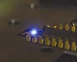
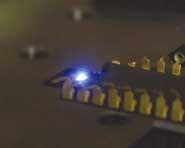
Because indium gallium nitride (GaN) light-emitting diodes (LEDs) have become so important in the areas of high-intensity illumination and large full-color displays, almost anything a researcher can do to improve their characteristics potentially carries great commercial significance. A group from the University of Strathclyde (Glasgow, Scotland) has developed a form of GaN LED in which an array of micro-LEDs is monolithically integrated with a microlens array. The largest benefit is a reduction in beam divergence without the bulky clear plastic lens package required for ordinary LEDs. The geometry should also enhance light-extraction efficiency.
In the prototype, the LEDs themselves were fabricated on a sapphire substrate and contain multiple quantum wells emitting at 470 nm into the sapphire. The array of microlenses was fabricated on the other side of the sapphire to match the array spacing of the LEDs. First, lithographically patterned photoresist disks were thermally reflowed, then dry-etched into the sapphire itself. The lenses are 20 µm high and 1.5 µm wide, with an array spacing on the order of 40 µm and a focal length of 43 µm. Greater than 80% of the light is emitted within an 80° cone. Contact Anthony Choi at [email protected].
Gold-doped HgCdTe detectors operate at high temperature
Researchers at DRS Infrared Technologies (Dallas, TX), SAIC (Albuquerque, NM), and the Air Force Research Laboratory (Kirtland AFB, NM) have developed mercury cadmium telluride (HgCdTe) IR detectors that have a high operating temperature of 130 K and a cutoff wavelength of about 5 µm. The IR photodiodes were fabricated on Hg1-xCdxTe samples with x approximately equal to 0.30. The devices were doped with indium (1 × 1014 cm-3) and gold (5 × 1015 cm-3).
Both 80-µm-thick planar diodes and 10-µm-thick cylindrical diodes were fabricated. The planar version is intended for rapid material characterization, while the cylindrical version, dubbed a high-density vertically integrated photodiode (HDVIP) by the researchers, is intended for staring focal-plane arrays. In development since the 1990s, the HDVIP in this version contains a conical flat-bottomed well surrounded by metallized semiconductor material. Both detector types showed good dark-current values, with the planar version reaching about 2.5 × 10⁻⁷ A/cm2 and the HDVIP showing 5 × 10⁻⁷ A/cm2, both at 130 K (much higher than the usual 77 K for HgCdTe detectors). In contrast, an older copper-doped HDVIP has a dark-current value of about 1 × 10⁻⁵ A/cm2 at 130 K. Contact Hung-Dah Shih at [email protected].
Transparent magnetic fluid has potential for optical devices
Magnetic fluids, which contain magnetic nanoparticles, have magnetic-field-dependent birefringent, chromatic, transmissive, and refractive-index properties that could make them useful in optical devices. One standard magnetic fluid contains maghemite (γ-Fe2O3) particles. Maghemite, however, has a low optical transmissivity, limiting its use in such fluids to those having low particle concentrations. Researchers at the Universidade de Brasília (Brasília, Brazil) are working with another magnetic fluid based on cadmium ferrite (CdFe2O4) nanoparticles, which are much more transparent.
In a comparison, the researchers created two different magnetic fluids in aqueous media, one of standard surface-coated maghemite, and one of passivated and peptized cadmium ferrite. A range of particle volume fractions was investigated for each fluid. Relative transmission measurements showed that the cadmium ferrite magnetic fluid was 17 times more transparent. Magnetic optical birefringence was also tested for the two materials at a sample thickness of 1 mm; the new magnetic fluid was 2.4 times as birefringent as the old. An observed negative differential characteristic in the intensity-vs.-field data of cadmium ferrite can be tailored by changing the sample thickness, particle volume fraction, or other characteristics of the experimental setup. Contact Paulo Cesar Morais at [email protected].
Nanostructured silicon diode shows stimulated emission
Approaches to creating a viable silicon laser—which would allow integration with standard electronics and make available the vast infrastructure of the integrated-circuit-chip industry—include porous silicon, as well as doping. Researchers at the Institute for Applied Science and Engineering Research and National Taiwan University (both of Taipei, Taiwan), California State University (Long Beach, CA), and the University of California (Irvine, CA) have developed an approach that relies on silicon dioxide (SiO2) nanoparticles embedded in a boron spin-on dopant. Experimental results show stimulated emission of light.
Mixed with dopant, SiO2 particles 4 to 20 nm in size were deposited on a silicon wafer and thermal diffusion performed to create p-doped layers (reference devices without the nanoparticles were also fabricated). The result was boron pillars 20 to 30 nm in diameter and 1 to 4 nm high, surrounded by regions of silicon oxides. Ridge waveguides with electrodes were fabricated. In contrast to the linear performance of devices without nanoparticles, the SiO2-laced devices showed superlinear increase in optical power with increasing current. Above a threshold current of 315 mA, the 150-nm spectral width of the output began narrowing; at 600 mA, two 3-nm-wide peaks at 1214 and 1217 nm predominated. Contact Chen Tsai at [email protected].
Single-atom-cooling method keeps atomic excitation low
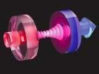
Researchers at the Max Planck Institute for Quantum Optics (Garching, Germany) have demonstrated a method for laser cooling of atoms that does not rely on repeated cycles of optical pumping and spontaneous photon emission. It relies instead upon photon emission from a high-finesse cavity excited from the left by a weak near-resonant probe field and a strong far-red detuned dipole field to cool single rubidium atoms injected from below into an intracavity dipole trap. A grating to the right of the cavity separates the two light fields and directs the probe beam to a single-photon counter.
The cooling achieved was estimated, at comparable atomic excitation, to exceed free-space Sisyphus cooling by a factor of five and Doppler cooling by a factor of 14. Unlike free-space laser cooling, the primary mechanism involves exciting the cavity portion of the strongly coupled atom-cavity system and achieves strong cooling forces while keeping the atomic excitation low. This characteristic may find application in systems—such as molecules without closed transitions and collective excitations of Bose condensates—that cannot be cooled by conventional methods. Contact Gerhard Rempe at [email protected].
Formula describes null-corrector sag and phase
A null corrector is a highly aspheric optical element that allows interferometric testing of large aspheric optics by correcting for the aspheric portion of their wavefront. If made inaccurately, a null corrector leads to an incorrect aspheric optic, as in the Hubble Space Telescope (before its expensive repair). Computer-generated holograms (CGHs) and diamond-turned mirrors (DTMs) are two forms of null corrector that can be accurately and straightforwardly fabricated. But because null correctors are located close to the ray trace's caustic region to reduce corrector size, modeling them with ordinary optical-design techniques is not possible.
Researchers at the University of Arizona (Tucson, AZ) have developed a mathematical formula to describe the sag and phase of null correctors to certify them; the formula has four to six terms depending on the degree of asphericity. The formula depends on a Shack surface, which deviates from sphericity to reproduce the normals of an aspheric test surface. Solutions for a DTM for a parabola and a CGH for a hyperbola show wavefront residuals of 0.001 waves (for comparison, the DTM defined instead with a polynomial has a residual of about 1000 waves). Contact Iwona Palusinski at [email protected].
Charge motion is optically imaged
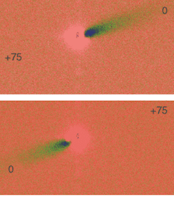
Researchers at the Naval Postgraduate School (Monterey, CA) and Fairfield University (Fairfield, CT) have developed a method of directly imaging the two-dimensional transport of free charge at the surface of planar semiconductor structures. The method relies on generating charge at a fixed point and imaging the luminescence caused by carrier recombination. Unlike cathodoluminescence, the new method preserves spatial information from the charge recombination, revealing charge motion due to carrier diffusion or drift.
A scanning electron microscope contains an optical microscope in its chamber; the incident electron beam passes through a hole in a mirror used to collect the luminescence. The optical system has a resolution of 0.4 µm per pixel. In one experiment, the researchers imaged the drift of holes in n-type epitaxial gallium arsenide. When 75-V biases of opposite polarity are applied across two contacts, corresponding drifts of charges can be seen. The approach permits direct observation of transport across contacts. The collected light could be spectroscopically analyzed to distinguish defect-related from band-to-band recombinations. The technique can be applied to any luminescent material. Contact Nancy Haegel at [email protected].
Single fixed laser crystal emits red, green, and blue light
A solid-state laser containing a single piece of active (gain) material that simultaneously produces red, green, and blue (RGB) light could be valuable for full-color image projectors. Typically, RGB laser light is produced by a complex arrangement of laser rods and nonlinear crystals. A version of single-crystal RGB laser has been developed by scientists at the Université Claude Bernard-Lyon (Villeurbanne, France) and the Chinese Academy of Science (Fujian, China) that relies on neodymium-doped gadolinium aluminum tetraborate (NGAB).
Pumped with pulsed light at 744.7 nm and 10-ns pulse duration (2.5 mJ per pulse), the laser operates at the dual wavelengths of 1062 and 1338 nm. Red light at 669 nm and green light at 531 nm result from self-frequency doubling of the laser's two wavelengths, while blue light at 480 nm results from self-sum frequency mixing of the pump and the 1338-nm laser light. All colors are emitted at the same time and at a fixed crystal orientation. For experimentation, a dye laser provided the pump light. The NGAB crystal was 4.9 mm long; for RGB output, phase matching was not exact for any of the colors. Contact Alain Brenier at [email protected].
Rectangular hollow glass tubes help 10.6-µm light stay polarized
Flexible, round hollow glass tubes coated inside with high-reflection coatings have been used to transmit high-power light beams from carbon dioxide (CO2) lasers for industrial use. The glass tubing material allows for conventional liquid-phase-chemistry methods for depositing the inner silver and silver iodide optical coatings. The round geometry of the tube, however, tends to depolarize the laser light. Because CO2 laser welding and cutting sometimes relies on polarized light, a different approach is needed.
Square and rectangular tubes transmit light with little polarization loss because of their perpendicular surfaces. Although metallic rectangular tubes for conducting 10.6-µm CO2 laser light have been fabricated, they haven't allowed for easy inner coating. Now, researchers from the department of ceramics and materials engineering at Rutgers University (Piscataway, NJ) have fabricated square and rectangular hollow glass tubes 1.25 m long that preserve up to 90% of polarization for 10.6-µm light and allow wet-chemistry coatings. The square tube has a 500 × 500-µm bore, while the rectangular tube has a 2.25 × 1250-µm bore. Attenuations were 0.8 and 2.2 dB/m, respectively. Twisting the tubes does not reduce polarization preservation. Some mode-mixing occurs from the slightly rounded tube corners. Contact James Harrington at [email protected].


