Silicon UV emitters are fabricated via CMOS
The quest to wring electrically produced light from silicon (Si) has resulted in several types of experimental emitters, including rare-earth-doped Si devices (see Laser Focus World, April 2003, p.‑19). Although none has been efficient enough for practical use, efforts continue, propelled by the dream of manufacturing vast amounts of inexpensive emitters by using computer-chip manufacturing processes.
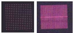
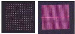
As well as trying to boost efficiency, scientists want to push Si-based emitters to shorter wavelengths. Researchers at the Institute of Ion Beam Physics and Materials Research, Forschungszentrum Rossendorf (Dresden, Germany) have demonstrated a relatively efficient electroluminescent Si emitter with an output that shows a sharp UV peak at 316‑nm-a wavelength useful for lighting, displays, biosensors, and fluorescence studies.1 Because standard CMOS technology is used, the emitters can be fabricated in sizes down to below 1 µm.
The devices are prepared on standard 4-in. Si wafers. The structure consists of a 100-nm-thick silicon dioxide (SiO2) active-gate oxide layer surrounded by 1-µm-thick field oxide. The SiO2 layer is implanted with ions of gadolinium at energies of 50 and 100 keV and doses of 5 × 10¹⁴ and 1 × 1015 cm−2 respectively. A 100-nm-thick indium tin oxide gate electrode is deposited by radio-frequency sputtering.
In operation under a high electric field, electrons are injected from the Si into the SiO2 layer containing the gadolinium ions by so-called Fowler-Nordheim tunneling, explains Lars Rebohle, one of the researchers. In this effect, the potential barrier the electrons have to overcome to enter the SiO2 becomes narrower and smaller as the electrical field is increased. If the applied electrical field is high enough a sufficiently high number of electrons are injected into the SiO2 layer.
Now in the conduction band, the electrons are accelerated by the applied electrical field, gaining kinetic energy. Under a constant electrical field, an equilibrium is reached in which the electrons have a constant average energy; under a high-enough electric field, the electrons reach an energy distribution with a maximum around 4 to 5 eV.
Some of the electrons scatter inelastically at the gadolinium ions, transferring energy to the ions and bumping them up to their excited 6P7/2 state. Their transition back to the ground state causes the emission of photons at an energy of 3.92 eV, equivalent to a wavelength of 316 nm. The process reaches an external quantum efficiency of greater than 1%.
Biochips
The low cost of CMOS manufacturing techniques will allow the Si-based UV emitters to be used in disposable products, says Rebohle. In addition, the other advantage of CMOS technology-the ability to pattern finely-make the emitters suitable for use in biochips that detect specific substances with fluorescence analysis.
A biochip typically contains an array of sample spots with either variably prepared surfaces to test one sample for different substances, or with uniformly prepared surfaces to test a set of different samples for the same substance. The substance under investigation is labeled by a dye, usually excited by a laser; the fluorescence is mapped either with a scanned detector or a CCD camera. In the latter case, the pixelation of data complicates the detection of low light intensities. In addition, an edge filter must be placed in front of the detection system to separate the laser light from the fluorescence signal.
If an array of small Si-based UV light emitters is used, the laser and the corresponding optical system are no longer needed, says Rebohle. Some biological substances can even be excited directly by the 316-nm light, eliminating the need for dye labels. Because the light emitters can be turned on and off individually, the instrument’s spatial resolution does not depend on cameras or scanning; instead, a single inexpensive large-area Si photodetector collects light. The detector integrates the signal, allowing much weaker light intensities to be detected. As a result, the fluorescence analysis can be performed with a setup considerably smaller in size-valuable for point-of-care diagnostics, explains Rebohle.
REFERENCE
1. J. M. Sun et al., Appl. Phys. Lett.(in press).

