Newsbreaks
InGaN-based surface-emitting laser has a horizontal cavity
Although it's not a VCSEL (vertical-cavity surface-emitting laser), researchers at NTT (Atsugi, Japan) and the University of Electro-Communications (Chofu, Japan) have created a surface-emitting indium gallium nitride (InGaN)-based blue-violet laser diode. Surface-emitting lasers, common in the red and infrared wavelengths in the form of VCSELs, are far easier to fabricate than edge emitters because they don't have to be cleaved. Ongoing efforts to create an InGaN-based VCSEL have not yet borne fruit. The Japanese researchers sidestepped the problem by fabricating a horizontal-cavity InGaN laser along with an angled mirror just beyond the end of the cavity.
The angled output mirror and the vertical cavity mirror are created by dry etching and selective regrowth of a magnesium-doped GaN layer; the mirrors are very smooth with little angular misalignment. The room-temperature, electrically pumped laser emits 0.3-µs pulses at 405 nm and a 1-kHz repetition rate. The output mirror lies at a crystal plane 58° from the vertical, so the beam is not vertical, but is emitted at an angle of 28° from the surface normal. The method enables wafer-scale fabrication of blue-emitting semiconductor lasers. Contact Tetsuya Akasaka at [email protected].
Terahertz QWIP responds at 42 µm
A terahertz quantum-well infrared photodetector (QWIP) with a response that extends below the optical phonon energy of gallium arsenide (GaAs) has been developed by researchers at the National Research Council (Ottawa, Ont., Canada) and the Chinese Academy of Sciences (Shanghai, China). Previously, absorption by GaAs optical phonons contributed to making the 36-µm and longer (9-THz and below) region of the spectrum inaccessible to QWIPs.
The aluminum (Al) content of the 40-nm AlGaAs barriers was kept to no greater than 5%; 50 12-nm-thick GaAs quantum wells completed the structure. Although the device still did not respond to a wavelength band between 34 and 39 µm, it did exhibit response at longer wavelengths, peaking at 42 µm. But, although theoretically the device should have reached background-limited infrared performance (BLIP) as its temperature was lowered to about 15 K, it did not; instead, at about 15 K the dark current stopped decreasing—an effect most likely the result of tunneling. The researchers will test wider and less-impure barriers to suppress the tunneling current. Terahertz QWIPs for even-longer wavelengths are in the works. Contact Hui Chun Liu at [email protected].
Odd-looking photonic-crystal-waveguide corner has low transmission loss
When optimizing a complex lens or thin-film-coating design, an optical engineer invariably resorts to the use of an iterative computer algorithm. Not only does this method save plenty of time, it also allows hundreds of variables to enter into the optimization, with a hoped-for result near the global optimum (and, for complex and demanding problems, producing a far better solution than an engineer could do otherwise). Now, this same approach has been taken in the design of photonic-crystal (PC) topology.
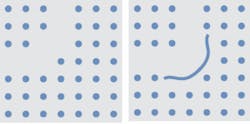
Researchers at the Technical University of Denmark (Lyngby, Denmark) used iteration to computer-design a 90° bend (right) in a 2-D PC that had a transmission loss of less than 0.3% across the entire frequency range of the guided mode, as compared to a conventional 90° bend (left) whose transmission loss was up to 9.0% in its frequency range. The model used a dielectric (black in figures) with a refractive index of 3.4; five dielectric posts in the corner were computer-reconfigured. Out-of-plane losses were not calculated—a step that requires a 3-D computer model. Contact Jakob Jensen at [email protected].
Ytterbium-doped calcium fluoride is gain medium for DPSS lasers
At the annual meeting of the Conference on Lasers and Electro-Optics (San Francisco, CA; May 16–21) researchers from l'Université Paris-Sud Center Universitaire (Orsay, France) and l'Université de Caen (Caen, France) reported a successful demonstration of ytterbium-doped calcium fluoride (Yb3+:CaF2) diode-pumped solid-state lasers yielding both continuous-wave (CW) and femtosecond-pulsed output. The pump beam was provided by a fiber-coupled laser diode emitting 15 W at 979 nm.
The lasing medium in the CW case was a 4-mm-long 5%-doped crystal, which yielded 5.8 W of output power at 1053 nm, as well as tunability from 1017 to 1072 nm. A similar lasing medium with a Brewster cut was used for pulsed operation. The shortest pulses achieved were 150 fs, centered at 1043 nm with 880 mW of average power; pulses of 220 fs with an average power of 1.4 W have been demonstrated. Once modelocked, the system was tuned from 1040 to 1053 nm and over a pulse-duration range from 200 to 440 fs. Contact Frédéric Druon at [email protected].
Quantum-cryptography keys traverse open air using single photons
In a post-deadline paper at the International Quantum Electronics Conference (San Francisco, CA; May 16–21), researchers from the Institut d'Optique (Orsay, France) and l'Ecole Normal Supérieure de Cachan (Cachan, France) reported successful implementation of the BB84 quantum-cryptography protocol in an open-air environment with single photons. BB84 consists of two separated individuals (normally referred to as Bob and Alice) who build and share a secret key using two communication channels, one quantum and one classical. Preliminary demonstrations of this concept were first achieved two years ago.
The recent achievement involved successful communication at night in the presence of city lights between two buildings at the Institut d'Optique. Single polarized photons in the 700- to 900-nm range were transmitted through open air (quantum channel) with the Internet serving as the classical channel. A secret-key distribution rate of 15 kbit/s was achieved and the device operated reliably in the presence of 12-dB attenuation. Contact Gaetan Messin at [email protected].
Negative-index planar silver lens images 250-nm features
Materials with a negative refractive index can be created from arrays of subwavelength resonant structures (a "metamaterial"), at least at microwave frequencies. A second approach, which works in the optical region, relies on the fact that some metals have a negative real refractive index for certain wavelengths; silver, for example, does at wavelengths not far from 341 nm. Light absorption is high, however, so only very thin films of metal can be used for optical experimentation.
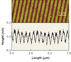
Now, a group at the University of Canterbury (Christchurch, New Zealand) has demonstrated a real-world use of negative-index optics by using a planar silver lens for 1:1 photolithographic imaging and patterning of submicron structures. A tungsten photomask, an 80- to 120-nm-thick silver lens layer, and a photoresist-coated substrate are spaced with 60-nm-thick transparent PMMA spacers. When exposed by a mercury-arc lamp, grating periods as small as 500 nm (250-nm lines and spaces) can be fabricated (simulations show that, when keeping the same geometry but eliminating the silver lens, no useful features would be created). The 500-nm-period grating shown here was created with an 80-nm-thick silver lens. Contact Richard Blaikie at [email protected]
Quantum-grid IR spectrometer forms pixel of focal-plane array
The field of imaging spectrometry may soon grow richer in the IR, if a single-pixel IR-spectrometer prototype developed by researchers at the U.S. Army Research Laboratory (Adelphi, MD) and Polytechnic University (Brooklyn, NY) is replicated into a 2-D focal-plane array. The pixel is a set of detectors called quantum-grid infrared photodetectors (QDIPs).
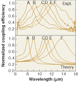
A grid is fabricated into a structure of aluminum gallium arsenide–based multiple quantum wells; metal strips on top of the grid scatter light into the wells. Each metal strip has a different width, selecting the peak detection wavelength of the structure beneath the grid. A prototype pixel with six QDIPs (A through E in figure) shows a peak coupling efficiency at a different wavelength for each stripe (top, measured; bottom, theoretical), spanning a broad band. "We are planning to rearrange the grid pattern into the shape of a daisy so that the center can be used for indium bonding, and the petals serve as multiprong optical antennas," says Kwong-Kit Choi, one of the researchers. "With this geometry, we are going to make the pixels as small as 18 × 18 µm in a focal-plane array." Contact Choi at [email protected].
Feroelectric domain patterns are directly written into lithium niobate
Another approach to fabricating polings with short periods in lithium niobate (LiNbO3) for use as nonlinear optical crystals has been demonstrated by researchers at Lehigh University (Bethlehem, PA). The Lehigh University group has developed a new technique in which ferroelectric-domain patterns are directly written onto a LiNbO3 wafer. In this technique, a field smaller than the one usually required for domain inversion is applied to the sample and a tightly focused 488-nm laser beam defines the positions at which the inversion takes place.
The origin of the effect is under investigation, but it is clear already that a space-charge field induced by the strongly inhomogeneous illumination and photoionization plays a major role in the process. The researchers found that the best results and smallest features can be achieved when the process is divided into two phases: domain nucleation and laser-guided growth of the domain. This crucial division of procession steps allows accurate control in the direct-writing method and is not possible in currently used methods. The patterns produced so far exhibit feature sizes down to 1 µm that appear to be limited only by the diffraction-limited spot size of the writing laser. Contact Volkmar Dierolf at [email protected].
Surface poling in lithium niobate waveguide creates efficient wavelength conversion
Used with red- or IR-emitting laser diodes, nonlinear crystals for frequency-doubling can result in a small blue-emitting laser that is a viable alternative to gallium nitride–based laser diodes. Periodically poled lithium niobate (PPLN) is a type of nonlinear crystal well known for this purpose. Researchers at the University of Southampton (Southampton, England) are using surface-domain inversion to create short-period (2.47-µm) periodic polings in waveguide versions of these crystals, resulting in efficient first-order quasi-phase-matched wavelength conversion.
Room-temperature photolithographic poling with an intentional "overpoling" step leaves small inverted domains under the photoresist-covered areas that maintain their original polarization states even when the rest of the volume has merged into one domain. An array of 12 waveguides separated by 100 µm and varying in width from 1.5 to 8 µm was fabricated and then poled. For a 825.2-nm pump wavelength (provided by a Ti:sapphire laser), the prototype 2-cm-long PPLN waveguide produced a second-harmonic (412.6-nm) power of 6 mW in the fundamental waveguide mode at a conversion efficiency of 7.4%, or a normalized conversion efficiency of 22.8%/W-cm2. Optimized devices will perform at a higher efficiency. Contact Alessandro Busacca at [email protected].


