Semiconductor ink advances flexible displays
Flat-panel displays are becoming increasingly popular alternatives to traditional cathode-ray-tube (CRT) monitors. Lightweight liquid-crystal displays (LCDs) offer mobility, and their thin size and small footprint allow them to fit more comfortably in many environments. In addition, active-matrix flat-panel displays are increasingly seen as a means to reduce energy consumption. According to the EPA, a typical color active-matrix LCD uses only 30 KWh per year (or 27 KWh per year with power management), versus consumption for a similar-sized CRT of approximately 135 KWh per year (70 KWh per year with power management).
Several factors hold back flat-panel displays from being pervasively present, however, with the most important being cost. While major strides have been made in large-area electronics over the past decade, the newest advances promise to make flat-panel displays, and future display technologies, even more cost-effective, and therefore more accessible and commercially successful. One advance that holds great promise is printed organic transistors.
Replacing silicon with plastic
The high cost of producing silicon-based backplane electronics is one of the factors that limit the economic production of large flat-panel displays. Although transistor backplane circuits for flat-panel displays do not require very high performance levels, they still require the same costly manufacturing techniques—the same sterile vacuum environment and the same high-temperature, high-vacuum, complex photolithographic fabrication processes.
Organic or plastic transistors have received great interest in recent years as low-cost alternatives to traditional silicon-based technology for electronic applications. This is not too surprising, as organic materials have already replaced inorganic materials in several devices, including photoreceptors, solar cells, and LEDs. Besides Xerox, Motorola (Schaumburg, IL), and Dow (Midland, MI), which work together to develop low-cost organic-transistor circuits, interested parties include academic laboratories at Stanford University (Palo Alto, CA), Penn State (State College, PA), and the University of Cambridge (Cambridge, England), and industrial R&D laboratories at IBM (Armonk, NY), Lucent Technologies (Murray Hill, NJ), DuPont (Wilmington, DE), Philips (Amsterdam, The Netherlands), and Siemens (Munich, Germany)—all have research activities dedicated to the development of organic-transistor materials and processes. The progress in this area has been great. Nonetheless, many challenges remain.
At the Xerox Research Center of Canada (XRCC) and the Palo Alto Research Center (PARC), we have developed new materials and techniques for the fabrication of organic electronic devices. These advances promise to make the production of large, flexible, lightweight displays not only possible, but far more cost-effective than existing silicon-based active-matrix displays.
Printed organic electronics
The technique being developed fabricates devices using high-volume inkjet printing to replace the photolithographic techniques used to create the thin-film-transistor backplane circuits used in displays. A liquid-based organic semiconductor material, developed by Xerox researchers, is used to print the semiconductor channel layers for large-area transistor arrays.
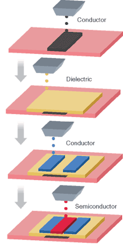
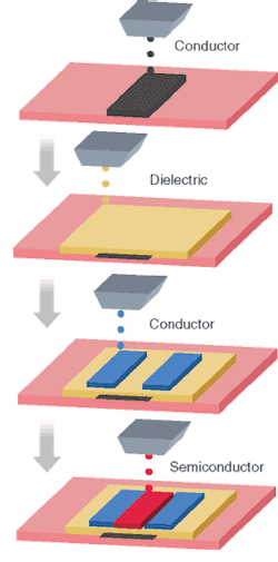
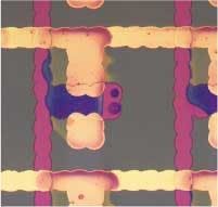
Current arrays are jet-printed using two techniques—an additive and a subtractive method—on either flexible or rigid substrates. The new polymer material dispersed in a liquid is jetted directly onto substrates just where they are needed—the additive process (See Fig. 1). Other materials are deposited everywhere and a mask is jet-printed on top. The material is then dissolved away except where protected by the printed mask—the subtractive process. In the future, we expect that all the layers will be printed additively using liquid-based conductors and dielectrics.
Both printing methods require precise layer-to-layer registration. The PARC printer is controlled by a computer-vision system to ensure proper alignment of the layers, even if the substrate warps or deforms during processing—a well-known complication with flexible substrates.
Recently, Xerox announced the development of three key components for fabricating low-cost organic-transistor circuits. These materials are liquid processable, and thus can be used to fabricate electrodes (source, drain, and gate electrodes), channel semiconductors, gate dielectric layers, and interconnecting lines in air for a transistor circuit using inkjet techniques. Thus, all of the elements necessary to make a plastic transistor circuit can now be inkjet-printed (see Fig. 2).
The materials challenge
The development of liquid-processable or printable organic semiconductor materials to enable fabrication of functional organic thin-film-transistor circuits under ambient conditions has proven to be very challenging. The transistor properties of liquid-processable polymers have tended to degrade when deposited in air, causing low mobility and low current on/off ratio. On the flipside, organic semiconductors with good stability in air generally require high-temperature vacuum-deposition techniques, making them unable to be fabricated through inkjet printing.
To solve this dilemma, a novel class of polythiophene semiconductor nanoparticles has been developed. These nanoparticles not only possess better air stability, but also exhibit excellent self-assembly behavior. Air stability is important because it will enable the semiconductor to be processed and fabricated into the transistor circuits in a manufacturing environment where stringent and costly environmental measures such as excluding atmospheric oxygen, moisture, and other atmospheric constituents are not required. In a liquid-processed organic-transistor semiconductor layer, proper molecular self-assembly leads to formation of molecular structural orders that are conducive to efficient charge-carrier transport, and thus high field-effect transistor mobility and faster transistor performance. High polymer field-effect transistor mobility to 0.2 cm2 V-1 s-1 and extremely high current on/off ratio to 10-8 have been obtained with Xerox's semiconductor ink.
Jet-printing plastic transistors
Fabrication of organic-transistor circuits using inkjet-type printing is expected to lead to many benefits. First, the technique is a low-waste process. Deposition and patterning are accomplished in the same step, reducing material usage and process complexity. In addition, inkjet printing can be accomplished using roll-to-roll processes and at various widths. This should lead to more process flexibility, higher overall throughput compared to batch processes, and lower overall costs.
We have succeeded in inkjet-printing organic-transistor circuits that matched the performance of those fabricated using spin-coating process. This demonstrates that inkjet-printing does not compromise the performance of the device. The organic transistors produced by the PARC scientists have exhibited exceptional performance, and meet most of the requirements for building active-matrix backplane circuits for displays, including high current on/off ratio, low turn-on voltage, good air stability, and very low current leakage.
Beyond having the ability to jet-print semiconductive polymers, the three liquid-processable materials could be used to create flexible plastic-transistor circuits using other common liquid-deposition techniques such as spin coating, screen or stencil printing, or offset printing.
Affordable wall-sized screens
Although current organic thin-film transistors do not have the high switching speeds or minuscule size of silicon transistors, they will be sufficiently useful for a variety of large-area electronic applications such as electronic paper and computer and television screens. While flat-panel displays are prohibitively expensive today, in the future printed organic electronics could make even huge wall-sized screens economically affordable and could be of great benefit to home entertainment as well as other display media such as poster and billboard advertising.
Printed organic circuits may eventually pave the way for products like thin, roll-up TV screens or 81/2 × 11-in. electronic paper that can be handled and treated like conventional paper.
BENG ONG is research fellow and manager, Advanced Materials and Organic Electronics Group, Xerox Research Centre of Canada, 2660 Speakman Dr., Mississauga, Ontario, Canada; e-mail: [email protected].