If there ever has been a field to raise confusion and suspicion in the photonics industry, it is nanotechnology, in which marketing may ultimately pose a greater challenge than the technology. The applications are diverse and mostly undeveloped, the opportunities are hidden all through the supply chain, and the timelines for products range from today to the distant future. And lurking behind all of that is the post-dot.com, post-telecom suspicion of “the next small thing.”
Without a doubt, there has been hype surrounding everything “nano.” But the hype has also been overhyped. Governments will spend more than $3 billion on nanotechnology R&D in 2004. Even if the definition of nanotechnology is loosely applied, that is real money. Moreover, nanotechnology is already in commercial products from sunscreens and stain-proof pants to nanophosphors and subwavelength optical microscopy.
What is nanophotonics?
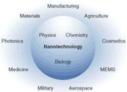
Nanotechnology is defined as a novel and multidisciplinary use of materials or processes at the nanometer scale (below 100 nm). So, the use of carbon nanotubes is clearly nanotechnology, but carbon black nanoparticles are not, because they have been used in products for more than 100 years. Nanotechnology involves mixing elements from the core fields of physics, chemistry, and biology to address other fields, and nanotechnology is also constantly finding new applications (see Fig. 1).
Nanophotonics is the use of nanotechnology in photonics, or the use of photonics in nanotechnology. A comprehensive list of nanophotonics companies would be too large to include here, but examples include Nanosemiconductor (Munich, Germany) and Zia Laser (Albuquerque, NM) in quantum-dot wafers, Evident Technologies (Troy, NY) and Nanosolutions (Hamburg, Germany) in nanocrystals and nanoparticles, Konarka (Lowell, MA) and STMicroelectronics (Geneva, Switzerland) in solar cells, NanoOpto (Somerset, NJ) and Little Optics (Annapolis Junction, MD) in photonic crystals and wires, and DuPont (Wilmington, DE) and Samsung (Seoul, Korea) in nanotube displays.
Particularly promising market opportunities for nanophotonics include improving the light output of high-brightness LEDs, reducing the manufacturing cost of solar cells, identifying better fluidic sensor solutions, and commericializing novel display technologies
Diverse supply chain
A bewildering and intermingled array of nanotechnologies and their applications arises because nanotechnology is not so much a thing as a process. The opportunities are often hidden in different levels of the supply chain.
Licenses. Many nanotechnology developments will improve on existing products through a process or a material. Revenues may come not from the sales of a product per se, but from royalties, or through sale of a license.
Materials. Much of nanotechnology is in materials science. Or, “Nanotechnology takes the complexity out of the system and puts it into the material.”1 Carbon nanotubes and titania nanoparticles are examples.
Components. Some nanotechnology developments will lead beyond mere improvements of existing products to novel components. Examples include photonic-crystal LEDs, quantum-dot infrared photodetectors (QDIPs), or nanofluidic sensors.
Systems. Few systems will be truly built around a nanotechnology, with revenues scaled to the value of the system. More often, nanotechnology will substitute for another core technology in an existing system product, such as a bioanalytical tool or optical networking equipment. An exception is in manufacturing tools that are used to make or inspect other nanotechnologies, such as nanoimprinting.
Setting reasonable expectations
It is common to see venture investors and start-up companies reaching as far as possible to capture revenues sized to components, or even systems. The “Intel Inside” brand is a reminder of the value of a high-performance component within a larger system. The large venture funds, especially, choose investments that offer potential for the largest returns. Too many investors are expecting blockbuster hits, however, and, the large venture investors are already expressing boredom with seemingly endless “nano” business plans for items such as nanosensors.
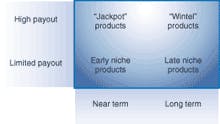
Seasoned entrepreneurs will look for opportunities all along the supply chain—opportunities that match their expectations for return on investment. Such entrepreneurs may be expanding their product line horizontally from their core business. Smaller funds and non-venture-funding sources are often better scaled to fit nanophotonics opportunities. Growth is slower, of course, so it takes a different personality and different skills to run such a business compared to a fast-growth startup seeking a “jackpot” success.Across the range of choices, some investors dream of “jackpot” products, or so-called Wintel products (see Fig. 2)—a Wintel product is one with high value and high volume, and dominant market share. Of course, the reality is that most products, if successful at all, will be niche products. Successful companies will scale their investments accordingly, and may have to live on government R&D funding, industrial partners, or debt financing for many years.
Multidisciplinary approach
A multidisciplinary marketing effort is especially important to find commercially viable applications. Electrical engineers, biologists, chemists, and other scientists don’t typically work together. People trained in these different fields speak different technical languages and look for different problems to solve. Universities set the example. Departments and publications revolve around traditional fields. Few academics get full credit for achievements in cross-disciplinary fields.
Integrating different disciplines to identify market opportunities takes time. Ideas need testing in the market, and the market infrastructure is not complete. The best opportunities may not come with the first merger of ideas, but after two or three generations of being passed back and forth within the market. If you think that nanotechnology is confusing, there is already talk of what will come after nanotechnology: the convergence of nano, biotech, information technology, and cognitive science. That new “meta-field,” or field of fields, is being called NBIC.
Overall, few companies in nanophotonics will succeed with jackpot products, but opportunities abound. To succeed, companies will have to be able to field a team of multidisciplinarians to develop new applications. They will have to look all along the supply chain, seriously considering licensing of processes or materials or sales of niche products. And, the companies will have to scale their investments and expectations accordingly.
REFERENCE
- Larry Bock, chairman of Nanosys, quoted in Small Times Magazine, July/August 2003, p. 30.
About the Author

Dr. Tom Hausken
Director, Photonics and Compound Semiconductor Products
Joining Strategies Unlimited in 1999, Dr. Hausken conducts the world’s leading market research in lasers and other photonics markets. He has nearly 30 years in the industry, including a joint project with Japan on optical computing while at OIDA, technology policy at the U.S. Congressional Office of Technology Assessment, and in R&D and production at Alcatel and Texas Instruments. He has a PhD from the University of California at Santa Barbara in compound semiconductor photonics.

