Because the subject matter covered by Laser Focus World is so broad, it is simply not possible to amass a comprehensive sampling of one year’s technical achievements in optoelectronics. One indication of this great quantity and variety of topics is the well-known lack of a single, universally accepted term under which all of them can be grouped.
“Optoelectronics” serves reasonably well, but to some it brings to mind transistors and capacitors. “Photonics” is closely tied to components and systems developed for the telecommunications industry. “Optics” suffices for some-to name two examples, the University of Rochester’s Institute of Optics (Rochester, NY) and the Optical Sciences Center at the University of Arizona (Tucson, AZ). But in fact, researchers at these institutions are involved in many technologies beyond systems of lenses and mirrors-which is what, for many, “optics” means.
Just as no one term covers the whole field, no one assorted selection of a year’s technical highlights can cover them all. Such an assortment can, however, at least serve as a nod to the quantity and quality of this year’s developments in the study and application of light.
Making monsters
One of today’s most interesting areas of basic research in optics is concerned just as much with electrons as with photons. When light interacts with structured metal surfaces, it can cause free electrons to oscillate in concert to form plasmons, which travel across the surface much in the same manner as light (see Laser Focus World, February 2004, p. 37). The field of plasmonics is involved with these effects, as well as with creating structures to best couple light in, propagate electron waves along the surface, and couple light out. The result may one day be plasmonic circuits that imitate what optoelectronic integrated circuits do, but at a much smaller scale.
Plasmon waveguides have been created; nanoscale arrays of gold dots fill the waveguide and are smaller in size near the edges of the waveguide (see Laser Focus World, May 2004, p. 28). Fresnel-zone-plate lenses can be fabricated of holey metal to take advantage of the properties of plasmons (see Laser Focus World, February 2004, p. 34). A near-field optical-lithography scheme relies on a photomask that converts light into plasmons and back (see Laser Focus World, August 2004, p. 32). It may even be possible to develop plasmon-gain elements, dubbed “plasmonsters,” which would enable regeneration of plasmons over the vast (in terms of plasmonic circuits) range of 1 cm (see Laser Focus World, November 2004, p. 32).
Photonic crystals grow more complex
The more established realm of research into photonic crystals (PCs) is yet to undergo a large-scale transition to commercial exploitation, but scientists and engineers are pushing PCs into ever more sophisticated territory. Photonic-crystal lasers have been developed, both in planar and surface-emitting form. A planar (2-D) indium gallium arsenide phosphide (InGaAsP) quantum-well PC laser has been created that contains two gain segments with a coupling region in between; the two gain segments are of slightly different lengths and produce longitudinal modes (frequency combs) with slightly different spacings (see Laser Focus World, March 2004, p. 44). Tuning one of these lasers by varying its current shifts its mode comb, so that when an element of its comb overlaps with an element of the other’s comb, a single strong mode appears. Shifting the comb again allows another spectrally distinct mode to dominate; the result is a tunable laser.
While 2-D PC emitters are relatively common, 3-D active PCs are not. Researchers at Kyoto University (Kyoto, Japan) have created a light-emitting 3-D PC by fusing a gallium arsenide (GaAs) PC substrate layer, an InGaAsP multiple-quantum-well emitting layer, and another GaAs PC layer.1 The fusion was difficult because of the differing thermal-expansion coefficients, so the researchers lowered the fusion temperature and lengthened its time. The resulting structure has a photonic bandgap at 1550 nm, with the bandgap suppressing spontaneous emission when the device is pumped with 900-nm light. A nanocavity-sized introduced defect strongly emits light (see Fig. 1). A future device with 17 layers should have a bandgap of less than 0.5 nm and a Q factor of more than 3000.
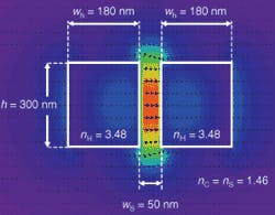
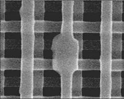
A form of optical waveguide that does not rely on either total internal reflection or reflection by interference (which is how PCs operate) was developed by scientists at Cornell University (Ithaca, NY; see Laser Focus World, February 2004, p. 15). With a low-index (1.46) core and high-index (3.48) cladding, it is based on a structure that creates electric-field discontinuities at the waveguide boundaries. This mostly wavelength-independent effect allows the use of waveguides only 50 nm wide (see Fig. 2). The small width and potentially high intensities make the waveguide ideal for stimulated light emission and nonlinear applications.Transcendent energies
With its 192 laser beamlines, the National Ignition Facility (NIF) at the Lawrence Livermore National Laboratory (LLNL; Livermore, CA) is driving toward its goal of creating break-even nuclear fusion for weapons experiments, basic science, future energy sources, and applied research (see Laser Focus World, January 2004, p. 42).
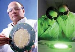
In “early light” testing, one of the NIF beamlines produced 10.4 kJ at the 355-nm wavelength that will be used for achieving ignition (see Laser Focus World, August 2003, p. 24). If all 192 beamlines perform as well, the resulting 2-MJ pulse should achieve ignition of a deuterium-tritium pellet. This initial system has since been taken offline for retrofit of a new generation of laser preamplifier modules (PAMs) being developed for NIF (see Fig. 4).Each PAM contains a high-energy laser amplifier with a pump chamber, a 32-mm-diameter Nd:glass rod, and power electronics to generate and discharge 12 kJ of pump energy to excite the laser rod. The rod diameter is large enough to allow four passes of the input beam. The 12 pulsed pump lamps in the PAM were custom-produced in a collaboration of Continuum (Santa Clara, CA), LLNL, and PerkinElmer (Fremont, CA); a high-efficiency diffuse reflector ensures uniform gain across the entire rod. For more information, see related article to be pubished in Laser Focus World, January 2005.
Fiber lasers enter the high-power arena
While many lower-power fiber lasers can be coupled into a single multimode fiber to create what is called a high-power fiber laser, the true frontier in fiber-laser development involves boosting the output power of single-mode (or close to it) single-fiber lasers. Here, the power limit is growing rapidly and has topped a kilowatt.
The first kilowatt-level fiber laser was created at the University of Southampton’s Optoelectronics Research Centre (Southampton, England), where researchers demonstrated a 1.01-kW output at a 1.09-µm wavelength and an 80% slope efficiency from a large-core 43 µm diameter) fiber with a numerical aperture of 0.09 (see Laser Focus World, June 2004, p. 9). The diode-end-pumped fiber had a D-shaped inner cladding of 650/600-µm size and a polymer outer cladding.
That level was soon pushed to 1.3 kW by researchers at the Friedrich-Schiller University and the Institut für Physikalische Hochtechnologie (both in Jena, Germany), who developed a D-shaped fiber with an extra fluorine-doped intermediate cladding to guide pump light (see Laser Focus World, August 2004, p. 36). The researchers believe that further scaling is feasible.
As for the sort of fiber laser that is in reality a combination of many, IPG Photonics (Oxford, MA) has pushed the output of these sources to 10 kW. The company is pushing its 5.5-kW version as a laser for welding in the automotive industry (see Laser Focus World, September 2004, p. 7). The source’s output can be delivered via a 100-µm-diameter fiber, the company claims. One form of competition for the IPG Photonics laser is a 4-kW diode-pumped solid-state disk laser introduced this year by Trumpf (Plymouth, MI); its output can be coupled into a 150-µm-diameter fiber, according to Trumpf (see Laser Focus World, September 2004, p. 19). The degree and rate of acceptance of the newer fiber-laser technology by the relatively staid automotive industry, as well as the long-term performance of the fiber sources, will determine which approach wins out.
Research on fiber lasers is taking many paths, including the development of Raman fiber lasers, coherently combined lasers, and improvements to femtosecond fiber lasers (see Laser Focus World, November 2004, p. 19). In one example, researchers at the University of Rochester (Rochester, NY) are using passive modelocking via a semiconductor saturable absorber in a colliding-pulse configuration with an ytterbium-doped fiber laser. Placed properly in the cavity, the saturable absorber produces 380-fs pulses at 605 MHz.
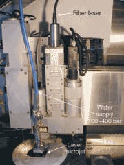
In one application of fiber lasers, engineers at Synova SA (Ecublens, Switzerland) use a water jet to guide laser light for materials-processing applications such as cutting silicon chips at rates up to 200 mm/s (see Laser Focus World, May 2004, p. S15). They had been coupling light from pulsed Nd:YAG lasers into an optical fiber with a 200-µm core diameter; the fiber projects into the water nozzle to deliver light to the water jet. Now, the researchers have taken the natural step of replacing the solid-state laser and coupling optics with a pulsed fiber laser (IPG Photonics; Oxford, MA) directly coupled to a delivery fiber with a 100-µm-diameter core (see Fig. 5). The smaller core produces a higher energy concentration, allowing the use of a thinner water jet. (For more on fiber lasers, see “Fiber lasers take off in diverse directions,” p. 81).Surpassing the eye, sort of
The human eye has on the order of 120 million optical sensing elements (rods and cones). Although aberrations in the eye lens, the brain’s role as image processor, and other effects cause the resolution of the human eye to be lower than this, the figure represents a target against which the resolution of optoelectronic imaging systems can half-facetiously be compared. In this vein, an astronomical imaging system built by e2v technologies (Elmsford, NY) can be said to outdo the human eye (see Laser Focus World, October 2004, p. S4). The imager contains 40 tiled back-illuminated CCDs, each with 2048 × 4608 pixels, for a combined pixel count of 377,487,360. The so-called MegaCam is in operation on a largefield telescope on Mauna Kea, Hawaii.
In reality, the human eye has qualities not found in any other optical instrument, including forms of image processing occurring at both the backplane (the retina) and in the brain, many details of which are only now being discovered. But, unlike even the most star-struck human, the e2v imager can stare at the sky all night without blinking and getting bored.
The application of CMOS sensors to high-speed imaging has found great success; for example, devices developed by Redlake MASD (San Diego, CA) provide high full-frame imaging (1504 × 1128 pixels at 1000 frames per second, or fps) and even higher windowed imaging (up to 100,000 fps). These imagers are used, for example, in the study of high-speed test automobile crashes, in which their antiblooming capability is a plus (see Laser Focus World, February 2004, p. 83).
For the consumer world, OmniVision Technologies (Sunnyvale, CA) has introduced a small-scale CMOS image sensor with 5 megapixels. The sensor’s small pixels—only 2.775 µm in size—allowed OmniVision to design the device with a footprint of a mere 0.7 in. The sensor is intended to match the image quality of CCDs of similar resolution and will be used in digital still cameras. The 2592 × 1944-pixel image array has an on-chip 10-bit analog-to-digital converter capable of operating at 4 frames/s in full resolution (QSXGA). Algorithms cancel fixed-pattern noise, eliminate smearing, reduce blooming, and minimize the effects of dark current.
Image is everything
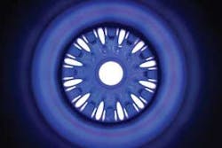
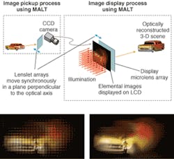
Having long ago clinched the laptop-computer-display market, the active-matrix liquid-crystal display (AMLCD) is adding desktop computers and television to its conquests. Variations on the technology continue to be developed. Nemoptic (Paris, France) is developing a bistable LCD with multiple gray-level control (bistable displays can be turned off and still retain their image—a feature that saves power even when they are on). Bistablility is achieved by controlling the position of a defect line inside each pixel by liquid-crystal backflow—the so-called “curtain” effect. Thirty-two gray-scale levels are possible—when combined with standard LCD color filters, a full-color (32K) display results (see Fig. 6). The company’s most recent version is a transmissive color display.A form of image display pursued by researchers at a modest level for decades—integral imaging—promises the portrayal of true 3-D images that one can peek around as if they were a real objects (in contrast to the more-common stereo 3-D-like images that “jump out” at the viewer but don’t offer differing perspectives). The technique uses ordinary incoherent light and arrays of microlenses, each lens capturing or projecting a different perspective (a bit like the small ribbed-lens novelty devices that, when turned, reveal a shifting scene). Unfortunately, integral imaging suffers from poor image quality. Researchers at the University of Connecticut (Storrs, CT) have developed a form of integral imaging that uses, along with the lens arrays, a CCD detector and flat-panel display for image capture and reconstruction, aided by a so-called “normalized computational 3-D volumetric reconstruction” algorithm.3
A toy car was imaged by the system (see Fig. 7). A 53 × 53-element pickup microlens array 55 mm on a side was placed 7 mm away from the closest part of the car. Each elemental image was 70 × 70 pixels. The flat-panel display, with another array, then projected the images. Most important, the pickup- and projection-lens arrays were moved simultaneously in a 2-D pattern to eliminate unwanted grid effects.Entering the everyday realm
While optical researchers are often content to create technology that betters their own particular experimental setup, or even the world of scientific and industrial optics as a whole, who wouldn’t get a thrill from seeing the results of his or her research plastered all over the home neighborhood? One optical material that may soon break free of the lab to find use in the everyday world is a coating developed by scientists at the University College London (UCL; London, England).4 The vanadium dioxide-based optical coating lets visible wavelengths through at all times but reflects IR light when the temperature rises above 29°C (84°F). The coating’s automatic switching ability may reduce room air-conditioning bills by up to 50%.
“While the heat-reflective properties of vanadium dioxide are well recognized, the stumbling block has been the switching temperature. It’s not much good if the material starts to reflect IR light at 70°C,” says Ivan Parkin, a professor of chemistry at UCL. “We’ve shown that it’s possible to reduce the switching temperature to just above room temperature and manufacture it in a commercially viable way.”
Vanadium dioxide’s properties are based on its ability to alternate between acting as a metal and semiconductor. The switch between reflecting or absorbing heat is accompanied by a small change in the structure of the material, in which the arrangement of electrons changes. Vanadium-vanadium bonds are stable below the transition temperature, locking the electrons and preventing conduction. Above the transition temperature these vanadium-vanadium bonds break and the electrons are free to conduct electricity, making the material metallic.
By varying the tungsten level, the researchers were able to show that the optimum concentration was 1.9%. To make the coating feasible to manufacture they chose atmospheric-pressure chemical-vapor deposition (APCVD), because it allows the film to be deposited during the float-glass manufacturing process and is performed at atmospheric pressure so no high-cost vacuum systems are required. The remaining problem is the coating’s unattractive yellow-green color, which the scientists hope to alter or suppress.
Dazzling LEDs
Another optoelectronic technology fast becoming more common in the consumer world is the high-brightness light-emitting diode (LED). Probably the most well-known white-light LED of this sort is the Luxeon, developed by LumiLeds (San Jose, CA). The emitter comprises a high-output chip mated to a heat-sinking substrate and encapsulated in silicone, with the phosphor coating applied directly to the chip (see Laser Focus World, September 2002, p. 17). White-light outputs reach 120 lumens for a 5-W version. Now, Cree (Durham, NC) is providing competition, in the form of its XLamp gallium nitride-based LED, which, unlike most LEDs, is fabricated on a silicon carbide substrate. The 1-W device provides 28 lumens of white light and is a surface-mount device that can be reflow-soldered, according to Norbert Hiller, vice president of lighting for Cree. Its ceramic substrate holds a copper heatsink and reflector; the LED’s optics are glass.
As is noted so often, the widespread use of white-light LEDs for general illumination is still years away, held back primarily by the devices’ high cost when compared to ordinary bulbs. But the term sometimes used by the industry for such a goal—the “holy grail”—illustrates the forward-looking approach that is propelling LED research at universities and industrial labs alike.
Lamina Ceramics (Westampton, NJ), for example, is packing LED chips in dense arrays with efficient heat removal, making possible a 27 × 32 × 2-mm device that emits 567 lumens of white light from 26 W of electricity (or, in a red version, 2045 lumens from 104 W). The emitter contains 39 cavities, each with multiple LEDs (see Fig. 8).The device takes advantage of a low-temperature co-fired ceramic-on-metal package that channels heat from the LEDs’ n-p junctions to the case with a thermal conductivity of 170 W/mK in the z direction and 220 W/mK in the x andy directions. The copper-molybdenum-copper substrate structure matches the thermal coefficient of expansion of the LED chips. The result is a postage stamp-sized lamp emitting as much light as a medium incandescent bulb.
Mounting large optics simply
Mechanical mounting is all-important to the performance of most optical systems. Some large optical systems have components that must be removed and replaced easily without altering the components’ positions or putting stress on the structure. One well-known approach to doing this is the three-point kinematic mount, which in its most basic form consists of two flat metal plates, one of which has three conical depressions into which fit three hardened metal spheres. The other plate has either a cone, a groove, and a flat area (the classic version) or three radial grooves (the simpler and more modern version); these areas also contact the same three spheres, locking the plates together while not putting stress on the plates.
One disadvantage of this type of mount is that the spheres only make point contact in the grooves, severely limiting the load the mount can bear. Engineers at G2 (Mountain View, CA), which designs and fabricates devices such as ultraprecise mechanical mounts and actuators for large telescopes, have come up with a simple way around this problem. They replace each sphere with an object that is half sphere, half cylinder (see Fig. 9); the spherical half makes line contact with the cone, while the cylindrical half makes line contact with the groove.Dubbed a Spherolinder, the kinematic component not only greatly increases the allowable load (the load capacity of a 1-in.-diameter mount increases from 20 to 2500 lb), but also permits smaller designs (for a 100-lb load, a 0.6-in. Spherolinder replaces a 7-in.-diameter sphere). The length of the cylinder is such that the line contact length for the spherical and cylindrical halves are the same.
REFERENCES
- Shinpei Ogawa et al., Sciencexpress, June 3, 2004, p. 1.
- F. Luan et al., Optics Letters, 2369 (Oct.15, 2004).
- Seung-Hyun Hong and Bahram Javidi, Optics Express, 4579 (Sept. 20, 2004).
- T. D. Manning and I. P. Parkin, J. Materials Chemistry, 2554 (Aug.10, 2004).
About the Author
John Wallace
Senior Technical Editor (1998-2022)
John Wallace was with Laser Focus World for nearly 25 years, retiring in late June 2022. He obtained a bachelor's degree in mechanical engineering and physics at Rutgers University and a master's in optical engineering at the University of Rochester. Before becoming an editor, John worked as an engineer at RCA, Exxon, Eastman Kodak, and GCA Corporation.
