Newsbreaks
Laser-diode frequency-doubling is simple and efficient
Direct frequency-doubling of electrically pumped laser diodes can lead to small and highly efficient sources of visible narrow-linewidth coherent light. But one advantage of laser diodes, their relatively low cost, is somewhat diminished by the complex (and therefore expensive) methods used for frequency-doubling. Researchers at the National Institute of Information and Communications Technology (Kobe, Japan) have refined the doubling process, simplifying it and lowering its cost while keeping it efficient.
A commercial extended-cavity laser diode emitting 50 mW at 1080 nm is combined with a potassium titanyl phosphate (KTP) cut in its "a" axis. The 1080-nm wavelength was chosen because it makes type-II noncritical phase-matching possible in KTP, which keeps both efficiency and second-harmonic beam quality high. Conversion to 540-nm light at 51.6% efficiency was demonstrated. Using resonant optical feedback, stable operation with a peak-to-peak intensity fluctuation of 0.3% over a two-hour period was achieved. An 82-kHz upper limit for linewidth was inferred from a Fabry-Perot measurement of the fundamental linewidth. As a first practical application, the researchers used the green light to pump a triply resonant continuous-wave optical parametric oscillator, generating quantum-correlated twin beams. Contact Kazuhiro Hayasaka at [email protected].
Changing pupil size does not affect task performance
It has been hypothesized that bright light sources help visual resolution partially by reducing the pupil size of the human eye and thus reducing the eye's optical aberrations. Scientists at the Lighting Research Center of Rensselaer Polytechnic Institute (Troy, NY) put the theory to the test on two groups, one with subjects aged 8 to 28 years and the other with subjects from 61 to 78 years, and found that the hypothesis is false.
The subjects examined charts of Landolt rings, which are broken circles commonly used to test visual acuity. The researchers tested subjects under four common office-lighting conditions using fluorescent lamps at two illuminances (500 and 344 lux) and two correlated color temperatures (3000 K and 6500 K). Each combination of illuminance and color temperature produced a different pupil size; both types of stimuli affected pupil size. Although a change in pupil size did not change acuity, greater illuminance for the same pupil size did increase acuity. The results also indicated that the 6500 K lighting was perceived as brighter than the 3000 K lighting at the same light level. Contact Peter Boyce at [email protected].
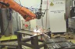
Fiber and disk lasers vie for attention in the automotive industry

Approaches to kilowatt-level industrial solid-state lasers include the fiber laser (multikilowatt versions of which are actually many individual fiber lasers with outputs channeled into one delivery fiber) and the disk laser (see "Commercial disk laser reaches 4-kW output," p. 19). Automotive manufacturers, some of which use kilowatt-level lasers for welding, are conservative in selecting laser types; for example, Volkswagen recently selected the disk laser over the fiber laser for sheet-metal-welding operations, at least in the short-term (see Industrial Laser Solutions, May 2004, p. 15).
The fiber-laser alternative, however, is evolving apace. In Burbach, Germany, IPG Photonics demonstrated a high-brightness (4.3-mm-mrad) 5.5-kW ytterbium-fiber laser to representatives of the European automotive and heavy industry communities; the company claims the output can be delivered via a 100-µm-diameter fiber. Operating at 1070 nm, the laser can be modulated to 20 kHz and has a wall-plug efficiency of 25% or greater. The high brightness allows a 1.4-m-focal-length lens to be used for remote welding. A unit was purchased by a major Japanese automotive customer and will be interfaced with a high-speed robot for remote production welding. Contact Bill Shiner at [email protected].
Ultra-low-index material helps photonic-crystal waveguiding
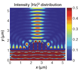
Two-dimensional slab photonic-crystal (PC) structures are often lithographically fabricated on a solid substrate—a configuration that reduces the difficulty of fabrication, but that also leaves only one very-low-refractive-index waveguide cladding, that between the upper PC surface and air. This configuration results in the waveguide modes extending deeply into the lower (solid) waveguide cladding, producing losses as well as mode asymmetries that cause coupling between TE- and TM-like modes. One solution is a membrane PC clad on both sides by air, but this form of PC is very fragile.
German researchers from the Technische Universität Hamburg (Hamburg), the Institut für Physikalische Hochtechnologie Jena (Jena), and the Max-Planck-Institut für Kohlenforschung (Mülheim an der Ruhr) have created PCs that rest on solid substrates of an ultralow-index material to create tight waveguiding and symmetric modes. Made of mesoporous silica, the substrate has a refractive index of 1.14; the researchers experimentally compared it to Teflon, which has an index of 1.3. Line-defect PC resonators with a polymer core were fabricated; improved transmission and symmetric field patterns were observed for the porous silica. Contact Markus Schmidt at [email protected].
Prisms are drawn, not ground and polished
Small prisms are often used in telecommunications and other optoelectronic devices. Researchers at Nippon Electric Glass (Shiga, Japan) are now avoiding the time, trouble, and expense of grinding and polishing such prisms by drawing them instead in a process similar to the creation of optical fibers. A glass preform is softened and drawn, with the preform's cross-sectional proportions staying the same even as the size is shrunk. Although the preform is only ground with a surface roughness of several microns, the as-drawn prism surfaces end up with high-quality optical surfaces.
For good temperature control in heating the preform, electrical heating is used. The researchers are currently fabricating 0.5 × 0.5-mm right-angle prisms with a dimensional tolerances of ±0.05 mm, angular tolerances of ±0.008°, flatness of λ/4, and a surface roughness of 10 nm. The drawn prisms, however, have rounded corners. Although they may reduce the clear aperture in comparison to ground and polished prisms, the rounded corners are flawlessly smooth, increasing the bending strength by about 50% compared to sharp-edged prisms. Contact T. Seto at [email protected].
Metallic nano-optic structures act like lenses
While the surface-plasmon-enhanced transmission of light through subwavelength apertures surrounded by metallic corrugations has been explored, metallic refractive-style nano-optics have not. Now, researchers at the University of Pittsburgh (Pittsburgh, PA) have simulated such optics through a finite-difference time-domain analysis. Their work shows the surprising effectiveness of these optics, at least in theory.
As is well known, a single subwavelength aperture (a slit, in 1-D) in metal diffracts light uniformly in all directions. If slits are brought adjacent to each other and spaced uniformly apart, however, and—most importantly—perpendicular thin metal walls are inserted between and outlying the slits (and the wall heights adjusted in particular ways to alter phase), refractive behavior results. For example, three slits with walls having linearly graded heights act together like a prism, sending the transmitted beam of light off at an angle. Bringing five slits together with walls having parabolically graded heights creates a functioning lens. Here, the slits are 80 nm wide and spaced by 400 nm; the structure receives TM-polarized 650-nm light and focuses it, producing a beam waist (the light is propagating upward). The arrangement is akin to phased-array antennas used in the microwave regime. Contact Hong Koo Kim at [email protected].
Optical-waveguide layer is integrated into electronic printed-circuit board
The fastest future computers will likely depend at least to some extent on optical interconnects for transmission of high-speed data between internal components (processors, for example). Researchers at the Universität Dortmund (Dortmund, Germany) have fabricated electronic printed-circuit boards with integrated optical-waveguide layers that are low in loss and can withstand typical solder reflow procedures. The multimode waveguides are fabricated of molded polysiloxane, which is the transparent material commonly used to encapsulate light-emitting diodes.
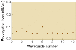
The mold was fabricated photolithographically and then electroplated. The 70 × 70-µm waveguide cores were then cast in the mold; next, a superstrate layer was cast atop the mold and the waveguides and superstrate removed. In the final step, a substrate was cast against the superstrate and waveguides, fully encapsulating the waveguides. After board lamination at 180°C for two hours and an annealing at 230°C for five minutes (to test temperatures reached by solder reflow), the waveguide loss was approximately 0.05 dB/cm at the commonly used 850-nm optical-interconnect wavelength. The casting technique allows micromirrors to be included at the waveguide ends for coupling in and out of the waveguides. Contact Andreas Neyer at [email protected].
Genetic algorithm boosts illumination uniformity in light guide
In designing a slab-shaped inverse-tapered light guide for a medical optical instrument, engineers at Bayer Diagnostics Manufacturing (Sudbury, England) found that the light guide's output strip emitted 50% more light at its center than its edges. To boost uniformity, the engineers decided to punch an aperture through the slab to direct some of the light from the center toward the edges. They quickly discovered that the precise shape of the aperture greatly affected uniformity in a relationship that was difficult to model analytically, so instead they used a genetic algorithm to determine the best aperture shape.
The 3.5-mm-thick acrylic light guide was 36 mm wide at the input end, 87 mm wide at the output, and 104 mm in length. Light-emitting diodes provided the illumination. A set of 500 apertures of random size and shape was generated, and physically impossible shapes weeded out. Using a macrolanguage in the Zemax (San Diego, CA) optical-design program, ray-tracing runs determined uniformity; random changes were introduced to the 16 best shapes and the procedure repeated. "Cross-breeding" by swapping some parameters between the best shapes introduced genetic variability. The resulting biconical shape reduced nonuniformity to 9%. Contact Juan Román at [email protected].
Subwavelength metal-semiconductor-metal gratings boost photodetection speed
At the Laboratoire de Photonique et de Nanostructures (Marcoussis, France), researchers are creating nanoscale (feature dimensions smaller than l/8) metal-semiconductor-metal gratings for ultrafast and highly efficient photodetection. Light in these subwavelength gratings is trapped via Fabry-Perot resonances involving vertical transverse magnetic surface plasmons and transverse electric guided waves.
Alternating silver and gallium arsenide wires are fabricated on an aluminum gallium arsenide spacing layer atop a multilayer Bragg reflector. The wires have a 40 × 100-nm cross section. The measured reflectivity of fabricated devices 10 × 10 µm in size for TE and TM polarizations matched well with theory, confirming the resonance mechanism. Photocurrent measurements at 780 nm show an external quantum efficiency (QE) of only 1% for TM polarization, far short of the 4% predicted by theory; the discrepancy is due to nonradiative defects. For TE polarization, a 9% maximum external QE is a factor of two less than theory. In the TE-polarization case, the small geometry of the detector should, with improvements in fabrication techniques, make possible a 500-GHz cutoff frequency in a photodetector with 75% efficiency. Contact Stéphane Collin at [email protected].