Stanford meeting highlights nanophotonics
The challenge for nanophotonics is not simply one of fabricating nanostructures, according to Frank Schellenberg, a strategic marketer for photolithography software at Mentor Graphics (San Jose, CA). Chemists have been creating nanostructures and dispensing them in beaker-sized quantities for some time. The challenge lies in positioning nanostructures where you want them and in having them do specific things.
Schellenberg made his comments during a nanophotonics panel discussion on the first day of the annual meeting of the Stanford Photonics Research Center (Palo Alto, CA). As usual, topics covered in the three-day multidisciplinary optics meeting ranged from the farthest reaches of fundamental optical sciences, such as quantum computing with linear optics, to everyday commercial realities, such as the technical challenges of meeting explosive consumer demand for cameras in cell phones.
So nanophotonics, a field in which fundamental enabling research continues at the same time as companies and products are beginning to appear on the market, seemed an apt topic choice for the annual industry panel session. Schellenberg, who sponsored several optical-proximity-correction (OPC) software startup companies while previously working with Sematech (Austin, Texas), discussed the challenges of nanophotonics from the perspective of semiconductor lithography in which techniques such as OPC, phase-shifting masks, and off-axis illumination enable the fabrication of circuit elements with feature sizes much smaller than the wavelength of light they are written with.
Optical-lithography manufacturing methods are not likely to extend much below 30 nm, despite the demand for even smaller components, he said. So the future of semiconductor manufacturing is likely to move toward hybrid fabrication methodology in which lithographic methods extend down to a threshold in the 30-nm region, and self-assembly of molecular or atomic-sized components builds upward toward the lower limits of optical lithography.
Subwavelength-scale devices
In a scientific presentation prior to the panel discussion, and again during the panel discussion, Harry Atwater, a professor of applied physics and materials science at California Institute of Technology (Pasadena, CA) discussed his work with subwavelength-scale optoelectronic devices that enable spatial confinement of light at dimensions less than 10% of the free-space wavelength, as well as propagation around sharp corners and through nanoscale networks, by exploiting the dipole-dipole coupling at the plasmon frequency between nanoscale metal particles in particle-chain arrays.
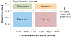
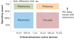
Resistive heating leads to relatively high losses during plasmonic transmission but very small device dimensions enable design tradeoffs of localization versus loss, as researchers pursue performance goals that include transport of light on a chip over distances on the order of a centimeter, he said. Long-term goals include design of subwavelength-scale optoelectronic components such as waveguides, sources, detectors, and modulators, as well as plasmonic gain components that Atwater calls “plasmonsters” and a recently developed field-effect-transistor-based light-emitting diode (see Laser Focus World, September 2004, p. 77). Ultimately, Atwater envisions localized power density and low-total-power plasmonic devices “that you can put in your pocket and power with a battery.” In a separate technical presentation, Rashid Zia, a graduate student in the Stanford laboratory of professor Mark Brongersma, characterized the potential of plasmonics for marrying the miniaturization of electronics with the speed of photonics (see figure).
Promising developments
Of the four panelists, Stan Williams, a senior Hewlett-Packard (HP) Fellow and director of quantum science research at HP Labs (Palo Alto, CA), drew the lion’s share of audience questions and commentary after he revealed the unfolding research and development strategy for nanophotonics at HP. Williams included photonic-bandgap materials, left-handed materials, nanostructure-enhanced Raman scattering, electromagnetically induced transparency, plasmonics, and entangled photons and teleportation in a list of both recent and promising photonic developments that are likely to have significant impact on application areas such as measurement, sensing, communication, processing and display.
The total attendance of 304 at the 2004 SPRC annual meeting included 150 industry professionals, 127 students and members of the faculty and staff of Stanford University (including the Stanford Linear Accelerator Center, Medical School, and other disciplines), 22 academics from non-Stanford universities and research centers, representatives from nine out of ten SPRC member companies, five representatives from U.S. government agencies, and international representation from Turkey, Japan, Germany, Portugal, Switzerland, Taiwan (ROC), and The Netherlands.

