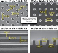
Nanostamps offer cost-effective nanoscale surface options
Surfaces textured at the nanoscale level have unusual chemical and optical properties for diverse applications in photonics, renewable energy, and polymer research and biochemistry. For companies unable to manufacture their own nanoscale-structured optical devices, Light-Smyth Technologies (Eugene, OR) offers a growing standard and custom library of “nanostamps”—nanoscale-textured surfaces patterned on single-crystal silicon chips.
Designed using CAD software, the patterns are translated into a mask using a laser writer and transferred onto silicon or glass substrates using high-fidelity, volume-friendly projection photolithography and reactive-ion etch processes. With substrates as large as 300 mm in diameter (but commonly 0.5 × 0.5 sq. in.), nanostructured feature sizes can range from 70 nm to several microns. Contact Dmitri Iazikov at[email protected].

