Synchronized modelocked pulses can create, then destroy electrons and holes
Synchronized modelocked pulses can create, then destroy electrons and holes
The first coherent destruction of photogenerated excitons in semiconductor quantum wells within a few hundred femtoseconds of their excitation has been demonstrated. Scientists from Hitachi Cambridge Laboratory and the Cavendish Laboratory, University of Cambridge, (Cambridge, UK) are working together on manipulation of carrier populations, which promises to remove some of the primary obstacles to realizing ultrafast optoelectronic devices and all-optical switching. The performance of such devices is currently degraded by long-lived carrier dwell times in the active regions.
Team member Albert Heberle says, OThe speed of present optoelectronic devices is limited by the time taken for electrons to disappear?usually about one nanosecond in semiconductors.O This time can be reduced to several picoseconds in extremely small semiconductor elements or in semiconductor materials that contain a high density of defects, but there are practical limitations to such approaches. OHowever,O continues Heberle, Oby employing synchronized light pulses, we have found we are able to generate and destroy electrons?an effect we call coherent destruction?on the time scale of our laser pulses, about 100 fs at present.O
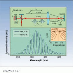
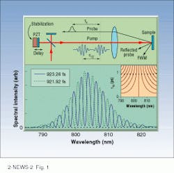
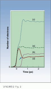
The researchers demonstrated coherent destruction by using phase-locked pairs of 100-fs near-infrared pulses. The first pulse creates electrons and holes, and the second following pulse is timed to destroy them. The success of this approach depends on accurately synchronizing the two pulses, which are created by splitting the beam from an ultrafast laser (see Fig. 1). The pulse pairs are routed to the semiconductor along different paths; controlling the path lengths thereby enables the pulse arrival times to be controlled (see Fig. 2). The two paths were stabilized to an accuracy of a few nanometers by using an arrangement of piezoelectric devices.
In the reported experiment, 70% of electrons and holes were destroyed within 200 fs. Further increases in the speed and in the fraction of carriers destroyed are expected in modified experiments now underway. At present, coherent destruction is observed at liquid-helium temperatures (?269!C) in very-high-quality GaAs quantum-well samples. The high-quality material and low temperature reduce the scattering of electrons and holes that causes loss of coherence. Future work is aimed at reducing these operating constraints. The team plans to further reduce scattering, for example, by using nanostructure devices such as quantum dots.
According to team leader Jeremy Allam the work establishes coherent destruction as a new operating principle for future optoelectronic devices. He notes that a lot more development must be done before practical devices based on this technology will be commercially available, but present results suggest that a new generation of coherent optically controlled semiconductor devices is possible.
Paul Mortensen
FIGURE 1. In experimental setup (top), modelocked Ti:sapphire laser
provides transform-limited pulses, from which two collinear pulses of variable intensity and temporal separation t12 are created by a computer-controlled Michelson interferometer. Active stabilization with a HeNe reference laser keeps t12 constant to 10 attoseconds for separations in excess of 100 ps. The pump and probe beams are separately acousto-optically modulated and subsequently focused to a 200-?m spot on
semiconductor sample containing five 12-nm GaAs quantum wells
separated by 12-nm Al0.3Ga0.7As barriers. Each pulse excites exciton
densities ranging from 10 to 12 cm?2.
FIGURE 2. Each laser pulse on its own excites electrons; the second pulse (b) is weaker than the first pulse (a). When both pulses arrive
in-phase, many more electrons are created (c). But with accurate adjustment of the timing of the pulses, the second pulse (indicated by the arrow) removes electrons from the semiconductor, producing coherent destruction (d).


