Optoelectronics research thrives in Europe

Optoelectronics research in Europe, as in other areas of the world, is a high priority and consequently a thriving research area. Research funding exists at both the national and European levels, and several major pan-European programs contribute to optoelectronics research and development. When devices become commercially viable, funding from industrial sources carries them through final development and into the market.
As an optoelectronic source, vertical-cavity surface-emitting lasers (VCSELs) are potentially low-cost devices for optical fiber communications systems and offer advantages such as on-wafer testing, effective fiber coupling, and array fabrication. The object of intense research in Europe, VCSELs also provide superior power efficiency and longer lifetime compared to existing devices. Furthermore, emission from VCSELs is perpendicular to the surface, which makes mounting the devices less demanding than mounting typical edge-emitting devices.
Research into blue-light-emitting diodes (LEDs) and diode lasers is also active. The gallium nitride (GaN) material system is one candidate for a blue-emitting semiconductor laser. The first European GaN Workshop, held in Rigi, Switzerland, in June this year, indicates the level of interest in this subject; the workshop attracted about 110 attendees, more than a quarter of whom were from Germany, 15% from France, and as many as 10% from Poland, which has a strong Group III-nitride research tradition (see Laser Focus World, Aug. 1996, p. 26). In addition, other researchers in Europe are successfully developing alternative materials for blue-emitting laser diodes.
Several world-class research groups throughout Europe are developing smart pixels, and this work is likely to expand as new funding becomes available under the European information technology program (ESPRIT). Applications of smart pixels include massively parallel processing in new computer systems, improved machine-vision systems, and fast switching in telecommunications systems.
As the optoelectronics research being undertaken within Europe is too extensive to review in complete detail, the representative developments described here will serve to illustrate the enormous scale and scope of the work.
At the Department of Information Technology (INTEC) of the University of Gent—which operates as a division of the Interuniversity Microelectronics Center (IMEC) in Leuven—about 120 researchers work in different fields of telecommunications including broadband and high-frequency communications and optoelectronics.
In-house epitaxial growth facilities enable researchers to fabricate a wide range of devices, such as laser diodes, LEDs, and other optoelectronic components. These devices are fabricated in arrays using simple processing schemes resulting in high reproducibility and high yield (see Fig. 1). The main emphasis of the department is telecommunications; thus the devices are based on gallium arsenide/aluminum gallium arsenide/ indium gallium arsenide (GaAs/ AlGaAs/InGaAs) and indium phosphide/indium gallium arsenide/ indium gallium arsenide phosphide (InP/InGaAs/InGaAsP) materials systems. The entire wavelength range from 750 nm to 1.7 µm can be covered with laser diodes having threshold currents between 1 and 10 mA.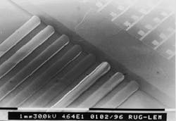
New structures are being developed using more-advanced growth techniques such as nonplanar and lattice-mismatched growth. The researchers have characterized a new vertical rotary reactor for multiple two-inch wafers and a new system for the growth of GaN materials. In the field of LEDs, INTEC currently holds the world record for external quantum efficiency—20%—of planar microcavity LEDs.
New projects include development of a multiple-wavelength laser for wave length division multiplexing (WDM) applications in collaboration with the Technical University of Delft (The Netherlands). The device is based on the integration of a phased-array wavelength demultiplexer with active gain sections; selective area epitaxy allows simultaneous emission of several wavelengths.
Another new project is assessing the potential of structured mirrors for VCSELs. Most VCSELs suffer from weak polarization and poor transverse mode stability, and the INTEC researchers hope the stability can be enhanced with a grating or other structured mirror. Their work has focused on the design of gratings with a high difference in zero order reflectivity for TE and TM polarization. Fabrication of VCSELs with such gratings is planned in collaboration with University of Ulm and EPFL-Lausanne.
Tampere University of Technology (TUT; Tampere) has a semiconductor research group of 25 scientists. Designated as a center of excellence by the Ministry of Education with annual funding of $1.5 million—derived primarily from business contracts—the group develops epitaxial compound semiconductor wafers and optoelectronic devices. A capital investment of $4 million in molecular beam epitaxy (MBE) growth systems, of which it has four, and state-of-the-art cleanroom facilities reflects the strategic importance of this technology to the Finnish government.
One of the developments emerging from TUT is production of aluminum-free GaInAsP 980-nm diode lasers that deliver up to 250-mW output power in a single spatial mode. Aluminum-free diode lasers offer significant advantages, including higher damage thresholds, reduced leakage current, and longer lifetime. Reliability testing of the TUT lasers indicates several thousand hours operation at high operating power. The laser beam shape has been optimized for pumping erbium-doped fiber amplifiers (EDFAs), and a fiber-pigtail-packaged module launches more than 100 mW of output power into a fiber.
Visible laser diodes are also produced at TUT. Red-emitting GaInP lasers provide a CW output power of 1 W from a shallow-ridge chip 40 × 1200 µm. Multiple-emitter diode-laser bars currently emit a maximum CW output power of 24 W with 38% wall-plug efficiency. The researchers have also demonstrated room-temperature operation of a pulsed ZnSe laser operating at 510 nm that was made using an "inverted doping" configuration (n on p). Although potential markets for such a system are promising, blue-green-emitting ZnSe-based lasers are still some way from commercial availability. Nonetheless, the TUT scientists believe they are one of the few groups worldwide that can overcome the problems involved in making reliable devices. To this end they have purchased a dual-chamber MBE system that will allow both III-V and II-VI materials to be grown in the same ultrahigh-vacuum (UHV) configuration without crosstalk between the chambers.
Visible-light microcavity surface-emitting LEDs (MC-LEDs) are also being developed. These devices are expected to emit a "super bright" laser-like output. The microcavity is a thin layer, on the order of a few wavelengths, sandwiched between two Bragg reflectors. Light is generated by quantum wells, either lattice-strained GaInAsP for red output or ZnCdSe for blue-green. The output linewidth of these sources is narrower than for a conventional LED, and the circular far-field pattern can be manipulated by modifying the surface to a much greater extent than is possible with edge emitters.
At the Institut d`Optique at Paris Sud researchers are trying to develop an artificial retina. They use smart-pixel technology to simplify an image before passing it to a computer for processing. The first processing step in computational vision—referred to as early or middle vision—involves interpretation of two-dimensional (2-D) images as projections from three-dimensional (3-D) scenes. By enhancing the image, reducing noise, and optimizing aspects such as edge sharpness the computing work necessary to complete image processing is greatly reduced, leading to orders-of-magnitude improvement in speed. One of the group`s more successful techniques is that of simulated annealing using laser-generated speckle patterns—the combination of speckle and dedicated integrated circuits being called a stochastic artificial retina. This opens the way for video-rate image processing in the pixel array.
The France Telecom Center National d`Etudes des Telecommunications (CNET) laboratories investigate devices, systems, and their implementation. The CNET optoelectronics materials and components group is located in Bagneux. One new development being pursued there is the possibility of fabricating hybrid polymer/semiconductor optical integrated devices. The goal is fabrication of a device with performance characteristics closer to those of individual semiconductor structures than is currently obtainable with monolithically integrated devices. At the same time production costs must be such that the hybrid devices can be used in real systems.
Among other devices under development at Bagneux is a new high-performance strained-layer integrated laser-modulator for 20-Gbit/s transmission. In this device, the same active layer provides for both a distributed-feedback (DFB) laser and modulator and is based on InGaAsP multiple quantum wells (MQWs). The laser emits at 1.553 µm, and performance tests demonstrated 20-Gbit/s transmission over 108 km of dispersion-shifted fiber. Such monolithically integrated laser-modulators are expected to be useful for long-haul transmission because of their compactness and intrinsically low chirp.
The researchers at Bagneux are also developing systems for millimeter-wave upconversion as part of a scheme for further development of distribution networks based on high-capacity microwave-radio systems over fiber. These systems are being developed rapidly worldwide for applications in areas including intelligent vehicles and information highways. Use of millimeter waves in radio communication systems will relieve spectral overcrowding while also supporting high data rates (622 Mbit/s). The optoelectronic upconverter developed at Bagneux integrates a MQW DFB laser with a distributed transimpedance microwave amplifier (DTA) on a single mount.
At CNET Lannion, researchers are investigating high-speed transmission over fibers and networks and also the overall architectures to optimize use of optical elements in networks. Working with the overall goal of introducing WDM in a synchronous digital hierarchy (SDH) telecommunications system across France and in a pan-European system, the group is developing time- and wavelength-multiplexing systems (T/WDM), SDH self-healing rings using optical add/drop multiplexers (OADM), and all-optical cross-connects based on wavelength conversion (see Fig. 2). Wavelength conversion is realized through a semiconductor optical amplifier (SOA), in which a counter-propagating low-power probe beam at the new wavelength uses the gain to take the signal characteristics from the original wavelength.
In Berlin at the Paul Drude Institut, fabrication of nanostructured semiconductors and synthesis of new materials by MBE is the basis of experimental work. In addition to investigating conventional quantum-well devices, superlattices, and differently doped structures, the institute is especially interested in applying ordering phenomena during crystal growth to develop novel structures. This work leads to a program rich in monitoring and measuring techniques. The institute is currently using such techniques to develop better ways of fabricating GaN-based LEDs and lasers. Deposition on both GaAs and silicon substrates is being examined in detail. There are also ongoing projects to develop multifilament current structures in n-GaAs for use in neural networks and to design and fabricate VCSELs.
The Universitat Ulm is home to one of the leading groups involved in the development of VCSELs, primarily in the spectral region between 800 and 1000 nm. The group uses solid-source MBE to fabricate multilayer systems on a substrate of n-GaAs. The active layer comprises GaAs with three strained In0.2Ga0.8As quantum wells in the center, and these produce light at 980 nm. Top and bottom mirrors contain Al0.7Ga0.3As/GaAs quarter-wavelength Bragg stacks. Current confinement is achieved either by using deep proton implantation or with selective oxidation of an extra AlAs layer directly above the top cladding layer.
To date, the best performance has been achieved with multimode oxidized 20-µm-diameter VCSELs; they produce 10-mW output power with a conversion efficiency of 47% and a maximum power of more than 40 mW. Continuous-wave operation is obtained from -80°C to +130°C. A single-mode laser produces 2.7 mW maximum output power with 50-dB sidemode suppression. Proton-implanted VCSELs are not as power efficient; the researchers found that oxidized devices are about three times as efficient as proton-implanted devices on the same wafer, although the latter devices do have low electrical capacitances that favor fast modulation.
One advantage of VCSELs is the ease with which fiber coupling is achieved. Butt coupling is a low-cost and simple solution. Low noise is crucial for good system performance, and this is usually characterized by a bit error rate figure (BER). For computer interconnects BERs of 10-12 or even 10-15 are specified. Laser noise control is thus essential, and optical feedback from downstream components can also be a noise source. The Ulm researchers have found that feedback sensitivity is reduced by using high-reflectivity output mirrors; feedback as high as -10 dB of the power does not produce a noticeable change in the BER noise floor when an output-mirror reflectivity of 99.8% is specified. The group has achieved data transmission rates of 10 Gbit/s with linearly polarized single-mode VCSELs over a 500-m graded-index fiber, with error rates below 10-12.
Working with Hitachi in Dublin, researchers at Trinity College, Dublin, are also using smart-pixel technology and have developed an optoelectronic retina that is used with a neural-network algorithm. Recent developments include demonstration of a fully optically addressed CMOS connected-component detector (CCD) chip. Whereas efficient photodetectors made in silicon have made the downloading of data onto a 2-D silicon chip relatively easy, it has been much harder to develop a system to download data off a CMOS chip. Full optical interconnection between chips allows faster information transfer by accessing the entire surface of the chip rather than relying on edge connectors, and this can be achieved without bandwidth penalty. The new system uses AlGaAs/GaAs MQW optical modulators, which also act as detectors, on prefabricated silicon-integrated circuitry, a technology offered by AT&T to academics last year.
Other areas of research necessary in neural-network design include examination of possible optical subtraction techniques. Lateral inhibition is the term used to describe the way in which cells in a sensory network affect near neighbors by suppressing their output. This is sometimes likened to a winner-takes-all situation—if one cell switches on, then adjacent cells switch off—and this improves the detectability of useful signals in a sensory neural network.
The Dublin groups have worked with researchers at Heriot-Watt University (Edinburgh, Scotland) to demonstrate use of self-linearized self-electro-optic-effect-device (SL-SEED) phenomena in this role. The system used in the demonstration comprises an absorption modulator in series with a photodiode, both based on quantum wells. When a voltage is applied across the wells, the absorption, and hence the intensity of the light incident on the layers, is modulated. Light incident on the photodiode can control the modulator current and consequently the modulator reflectivity. The reflected signal from the modulator is proportional to the difference between the light falling on the modulator and that falling on the photodiode, that is, it acts as an optical subtractor and can switch off cells. Large-device arrays can be integrated monolithically or with silicon circuitry for increased functionality.
The Laboratory of Photonics and Microwave Engineering at the Royal Institute of Technology (KTH; Stockholm), carries out research into photonics and high-speed electronics, combining these into optoelectronic integrated circuits for communications systems. Recent advances include development of a monolithically integrated receiver based on an InP chip and having a bandwidth of more than 20 GHz. Included in the system is a heterojunction bipolar transistor (HBT)-based preamplifier. Although the 20-GHz bandwidth would allow simultaneous transmission of about half-a-million phone calls, the project goal is to extend the bandwidth to 30 GHz.
The laboratory is also building new laser systems, and both high-speed and widely tunable diode lasers have been produced. Recent results show a bandwidth exceeding 26 GHz for 1.55-µm InGaAsP/InP DBR lasers and 24 GHz for DFB lasers. Indium phosphide lasers tunable over 100 nm have also been produced, offering the potential for terahertz bandwidth in fibers.
The research also includes vertical-cavity lasers. Although GaAs-based VCSELs operating at about 1 µm have been developed quickly, progress with the longer-wavelength devices required for communications has proven more difficult. The KTH group, however, working with Ericsson Components (Kista), has demonstrated a 1.53-µm laser based on one GaInAsP/InP mirror and one Si/SiO2 mirror in combination with a strain-compensated GaInAsP quantum-well active layer. The device operates pulsed at room temperature and in fact will operate over the range from -160°C to +43°C. The threshold current is 10 mA at room temperature. Continuous-wave operation was achieved up to -25°C. Maximum power is about 90 W at -60°C. The group expects to improve performance by matching the cavity mode to the gain peak and hopes to develop this into a room-temperature CW device.
At Chalmers University (Goteborg), the Department of Optoelectronics is focused primarily on components for the communications industry. Optical fiber nonlinearities are being investigated for high-speed transmission links. This includes various dispersion-compensation techniques and all-optical manipulation of data at high bit rates using the nonlinear optical loop mirror. This work will form part of an ACTS project called MIDAS.
In terms of devices, the group is studying surface-emitting lasers, both VCSELs and grating-coupled surface-emitting lasers (GCSELs) but with an emphasis on the latter. Research includes the use of computer-generated waveguide holograms to replace external beam-shaping optics (see Fig. 3).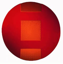
Monolithic integration of all-optical components enables fabrication of microsensors that are very robust. The Paul Scherrer Institut in Zurich is developing diode-laser-based optical devices and circuits for sensors and metrology. The institute`s work involves fabrication of custom diode lasers for each sensor application and is done in collaboration with several different industrial partners.
As a demonstration of the possibilities of OEICs, the Zurich group fabricated displacement sensors, one based on a Michelson interferometer and one on a Mach-Zehnder interferometer. With a distributed-Bragg-reflector (DBR) laser emitting at 820 nm, 49 fringes were seen for a displacement of 20 µm, with good fringe visibility at small measurement distances. Another sensor already tested is a refractometer optimized for high sensitivity in immunoassay applications. This device uses a Mach-Zehnder interferometer with a TiO2-on-SiO2 waveguide as a sensor pad in one arm of the interferometer (see Fig. 4).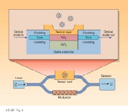
With central laboratories in the Netherlands and others throughout Europe and in the USA, Philips is one of the world leaders in optical information storage. The company is also involved with diode-laser development, solid-state imaging systems, and telecommunications.
At Philips Imaging Technology in Eindhoven the world`s largest CCD-based image sensor was produced earlier this year. The single integrated circuit contains more than 66 million pixels in a device measuring 86 × 110 mm. A new production philosophy made the device feasible; modules of pixels—an array of 1024 × 1024 12-µm elements—are produced by a standard mask and then repeated as necessary to produce larger and larger sensor arrays. Production runs can, therefore, move smoothly from large to small sensors, all being multiples of the basic module. For units where the high sensitivity of the 12-µm pixel is not required, the pixels are combined to form larger units on read-out. Applications for large-area sensors include medical imaging and astronomy.
Among the plethora of research work being undertaken on diode laser sources at Philips is a project building compact violet-emitting (426-nm) lasers—the shorter wavelength allows higher storage densities in optical recording. The new system is based on an AlGaAs laser specially configured and produced within Philips that is frequency doubled in a periodically poled KTP waveguide. The most-compact version of the prototype laser is just 1 × 1 × 2 cm and produces an output power of 85 µW, with a pulse-repetition frequency of 940 MHz, at room temperature (see photo). Higher-power versions, using optical feedback to enforce a single spectral mode in the laser, produce up to 0.5 mW in a device about 7 cm long.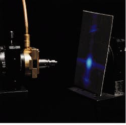
Recent work from the physics department at Vrije University (Amsterdam, the Netherlands) demonstrates a new technique for making switchable mirrors. A group headed by Prof. Griessen has used, as the basis for a switch, the change in optical properties that accompanies a transition from metal to insulator, or semiconductor, in rare earths and their hydrides.
The materials first studied were yttrium and lanthanum hydride. The bulk materials are unsuitably fragile, so a mirror was made by coating thin films (typically 500 nm thick) of the rare earths under ultrahigh vacuum. The resulting film was covered with a thin (5-20 nm) layer of palladium to prevent oxidation. The palladium does, however, allow hydrogen to pass through. Checks on the electrical properties of the YHx (0 < x < 3) films produced showed behavior similar to the bulk samples.
The group demonstrated reproducible and reversible changes from the metallic yttrium to the still-metallic YH2 to the insulating YH3 as the pressure of hydrogen gas surrounding the sample at room temperature was increased from 0 Pa to about 105 Pa. The transition is from shiny, fully reflecting pure yttrium to partially reflecting dihydride and then to a yellow transparent trihydride window. The actual transition from reflector to transmitter happens on a change in hydrogen loading that takes just a few seconds to achieve (see Fig. 5). Absorption edge measurements show that the gap energy is 1.8 eV, with an absorption edge up to 2.8 eV.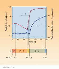
Prof. Griessen believes that transitions can be made to operate at higher speeds by using other rare earths and by finding an electrochemical means to drive the transitions. Work has already been done using mirrors based on the hydrides of alloys, and this will form the basis of patents. The group hopes that this effect will be utilized in a commercially viable family of devices.
Representing one the largest research group in Scotland, the Scottish Collaborative Initiative in Optoelectronic Sciences (SCIOS) is led by the Department of Physics at Heriot-Watt University, Edinburgh, and focuses on the applications of optoelectronics in high-performance information-processing systems (optical computing). Other organizations in the consortium include Glasgow University, Edinburgh University, and St. Andrews University. Areas of expertise include optical-processing systems, semiconductor fabrication, spatial light modulator (SLM) technology, and diode-pumped solid-state laser design.
Milestones within SCIOS include the first S-SEED arrays capable of working with Nd:YLF laser illumination at 1047 nm, which have been fabricated with MBE-grown strained InGaAs/GaAs structures. This work has been taken further by developing hybrid InGaAs/Si smart-pixel arrays. Smart pixels combine the advantages of optically interconnected logic elements with the processing power of silicon circuitry. This allows construction of effective 2-D arrays of optoelectronic processing elements.
One example of this is a recently developed electrically addressed SLM comprising a strained InGaAs optical modulator array, developed at Glasgow University, that is flip-chip-connected to a CMOS control backplane developed at Edinburgh University. Read-out is accomplished using a Nd:YLF laser, developed at the University of St. Andrews, with diffractive optics and a compact optomechanical assembly developed at Heriot-Watt University.
At the end of this year the SCIOS project members expect to have built a demonstration system. An optoelectronic sorter, based on the CMOS/InGaAs smart pixels al ready developed, is expected to sort 1024 16-bit words every 10 µs. Such parallel optical systems have the potential of significantly outperforming all-electronic systems and open up the prospect of powerful new computer architectures.
Heriot-Watt University is the lead partner in a new ESPRIT project covering smart-pixel optoelectronic connections. Designated SPOEC, the project will develop another demonstrator, this time an optoelectronic crossbar. Other partners include the University of Glasgow, SUPELEC (Metz, Paris), Trinity College, Dublin, and the Paul Scherrer Institut, Zurich, which will provide the expertise on VCSELs and VCSEL arrays.
Smart-pixel SLMs
At Cambridge University, the Northern Telecom Research Professor of Photonics and his group are involved with many projects of interest to optical communications and of more general interest. Much of the work involves SLMs based on ferro electric liquid crystals (FLCs). One device developed for telecommunications applications is a smart-pixel FLC SLM intended as an input device for an optical ATM switch. Research has shown that the standard thinking in optical switch architectures can be adapted to an ATM switch by using multistage switching. Combination of optical and electronic switches makes possible quick and efficient routing of ATM packets. This new chip is called opto-RAM because it appears to the system electronics as standard RAM (random access memory) but can be read optically.
Ferroelectric liquid-crystal SLMs have also been used in holographic switch architectures. They can display binary-phase holograms that allow a beam to be steered in a Fourier optical system. Such a mechanism forms the basis of a holographic switch where light is steered from input fibers to output fibers.
Another device developed at Cambridge, based on as yet unpublished work, is a 320 × 240-pixel fast-bitplane SLM, capable of displaying images at 2000 frames per second (see Fig. 6). Based on a VLSI silicon backplane array of mirrors, the device is fabricated as a standard CMOS VLSI wafer, then post-processed to include a ferroelectric liquid crystal to modulate the light.
A novel spin-off project has been development of a robust and flexible 3-D video display system. A ferroelectric liquid-crystal shutter spatially filters the Fourier transform of an image from a standard cathode ray tube (CRT). Sixteen different views of the object are created by multiple cameras, and the shutter forces the sixteen views into sixteen adjacent directions at the observer`s side. With so many views an observer sees a stereoscopic image from a range of positions, so a head-tracking system is not necessary.
Fabrication of a CdxZn1-xS/ZnS laser diode for use in optical storage applications is the goal of a research project at the University of Hull. Doping studies of the material are being carried out, and the project recently reported UV lasing at 333 nm—believed to be the shortest lasing wavelength yet reported from a semiconductor heterostructure. Re searchers observed the laser action in ZnCdS/ZnS stacks grown by MBE on GaP; the device was pumped at about 315 nm by a frequency-doubled-pumped dye laser.
The materials are characterized by the level of cadmium doping within the structure, as noted by the "x" in the formula. Lasing in the structure with the lowest cadmium composition (x = 0.03) gave the shortest output wavelength, 333 nm at a temperature of 8 K. Higher cadmium doping produces longer wavelengths and operation at room temperature. A composition of x = 0.20, for example, emits at about 360 nm at 8 K and 376 nm at 300 K; the threshold at room temperature, however, is more than one order of magnitude higher than at 8 K. The researchers` analysis indicates that an electronic gain contributes to lasing.
Fiber laser research
In what is believed to be the first demonstration of laser action in a rare-earth-doped chalcogenide glass, researchers at the Optoelectronics Research Centre of Southampton University have reported a Nd-doped gallium lanthanum sulfide (GaLaS) laser operating CW at a wavelength of 1.08 µm when pumped with a Ti:sapphire laser at either 815 or 890 nm. In addition the researchers demonstrated, for the first time, fabrication of GaLaS optical fibers—core-clad fibers longer than 200 m were made (see Laser Focus World, Aug. 1996, p. 25). These two developments are the first steps towards realization of fiber lasers operating at new wavelengths. The Southampton group hopes to optimize the system by changing doping concentration and configuration of the laser.
Continuing constant pressure from industry, governments, and consumers for higher-capacity—and faster—data and voice links, increased computing power, more data storage capacity, and better image processing will doubtless push the pace of optoelectronic development to ever increasing heights, not only inside Europe but throughout the world.