1999 TECHNOLOGY REVIEW: Optoelectronics moves forward on many fronts

The demands and desires of the everyday world do nothing less than a world of good for optoelectronics. The success of flashy consumer toys, information technology spurred by computers and the Internet, and medical advances link researchers with businesspeople and thus further nourish the market. This big-business side of optoelectronics has made possible the proliferation of complementary-metal-oxide-semiconductor (CMOS) imagers and fiberoptic components for wavelength-division multiplexing (WDM) and will soon usher in the widespread use of micro-optomechanical systems (MOEMS). Gallium nitride-based light emitters are the subject of continuing study, as researchers look for the key to bringing their costs down. Near-field optical systems show potential for high-density data storage and may one day find a place in the personal computer.
Open-ended research yields rewards, as well. The ultrafast laser is causing what can only be called a revolution in a range of disciplines ranging from chemistry to materials processing. Photonic crystals are expanding in capability. New lasing mediums for diode-pumped solid-state (DPSS) lasers promise simplicity of construction and additional wavelengths. Following are some of the past year's highlights in optoelectronics arising from both the commercial and academic arenas.
Ultrafast wins a prize
Combining peak pulse powers up to the terawatt level with modest average power and size, ultrafast (UV) lasers bring plasma physics into the optics laboratory—and potentially onto the factory floor. The near-infrared-emitting femtosecond Ti:sapphire laser dumps energy into its target so fast that matter has no time to dissipate heat, but instead becomes a quickly ejected stream of ions. The laser's high intensities have allowed researchers to create thermonuclear fusion (see Laser Focus World, June 1999, p. 24) and enrich isotopes (see Laser Focus World, Nov. 1999, p. 15) using experimental setups that fit on an optical table. The brevity of the UV laser's pulse has set into motion an area of physical chemistry called "femtochemistry"—pioneered by researcher Ahmed Zewail (California Institute of Technology; Pasadena, CA) for which he received a Nobel prize in chemistry this year.
Femtosecond pulses remove material with no recasting, slagging, or heat damage—a property exploited by Clark-MXR (Dexter, MI), a developer of UV laser systems. The company has introduced the first commercial femtosecond micromachining workstation, which contains computer-controlled translation stages as well as the laser and optics. The laser itself produces 0.8-mJ, 150-fs pulses of nearly TEM00 beam quality at a 1-kHz repetition rate.
Because the technology is so new, the first use of the workstation will be for research into potential industrial uses, according to Bill Clark, president and chief executive officer of Clark-MXR. "It's a means of getting into the technology quickly for people who are not laser jocks, but who are familiar with the industrial environment," he says. Along with micromachining such difficult materials as Invar, a femtosecond laser can directly form single-mode waveguides in transparent glass by a process of confined multiphoton absorption and avalanche ionization—a use being pursued by Clark-MXR.
Thanks to the diode
Diode-pumped solid-state lasers of all types continue to grow more powerful, as well as to diversify in output wavelengths. The optical output of the highest-power commercial diode-pumped Nd:YAG laser made by Rofin-Sinar Laser GmbH (Hamburg, Germany) has reached 4.4 kW; the laser has a beam parameter of 12 mm-mrad, and its light can be coupled into a 300-µm-diameter optical fiber. TRW (Redondo Beach, CA) has built a series of diode-pumped Nd:YAG lasers including versions emitting up to 6 kW; a 3-kW version cuts 0.5-in.-thick titanium at a speed of 90 in./min and 1-in-thick nickel alloy at 2.5 in./min.
A 1.7-kW version will become the central component of a light source to be used for extreme-ultraviolet lithography by EUV LLC, a consortium of US semiconductor manufacturers. Now installed at Sandia National Laboratories (Livermore, CA), the source will produce 13.5-nm light as the laser beam interacts with a xenon jet to create a plasma.
When combined with nonlinear optics based on stimulated Raman scattering, DPSS lasers can produce hundreds of wavelengths (see Laser Focus World, Nov. 1999, p. 137). A group of researchers at Osaka University (Osaka, Japan) has demonstrated noncritically phase-matched second-harmonic generation of a Nd:YAG laser in the nonlinear material GdYCOB at room temperature, with phase-matching possible for both second- and third-harmonic generation.
Insensitive to angular and temperature variations, the material is an attractive candidate for practical applications. Ultraviolet-emitting DPSS lasers with 355-nm optical outputs at the watt level are valuable for laser marking and semiconductor processing and are now being produced by Light Solutions (Mountain View, CA), Coherent (Santa Clara, CA), Quantronix (East Setauket, NY), and others. A 355-nm DPSS laser made by Photonics Industries International emits 7 W of light with TEM00 beam quality; a 266-nm version emits 2 W, also of TEM00 quality. The outputs of DPSS lasers will continue to rise dramatically over the next year.
The commercially available gallium nitride (GaN) based, blue-light-emitting semiconductor laser developed by Shuji Nakamura of Nichia Chemical Industries Ltd. (Kaminaka, Japan) remains at low power (5 mW) but has found its way into commercial products such as diode-laser modules produced by Coherent Auburn Group (Auburn, CA) and Power Technology (Little Rock, AR). Because the laser can be tuned over a 2.5-nm range and is available with a center wavelength of 390-410 nm, it has been incorporated into a spectroscopic system built and marketed by TuiOptics (Munich, Germany) intended for fluorescence detection and other applications (see Laser Focus World, April 1999, p. 69, and Sept. 1999, p. 57).
Although GaN-based green-, blue-, and UV-light-emitting diodes (LEDs) were pioneered and first commercialized by Nichia, other sources of this important product have appeared. These include Roithner Lasertechnik (Vienna, Austria) and Cree Research (Durham, NC). The LEDs made by Cree consist of an indium gallium nitride (InGaN) active element on a silicon carbide (SiC) substrate—an outgrowth of the SiC semiconductor technology that has for 12 years been Cree's bedrock business. Cree is heavily involved in the development of InGaN-on-SiC blue-emitting lasers as well and has entered into an alliance with Microvision (Seattle, WA).
A maker of microdisplays in which raster-scanned light is projected directly onto the eye's retina, Microvision needs Cree's devices to achieve both full color and compactness. Integrated Photomatrix Inc. (IPI; Hilliard, OH) circumvents the bulk of LED cans and builds the LED chips themselves into arrays used for scanning, illumination, and other purposes. With Nichia as a source of UV LED chips, IPI is extending its array capability to UV.
WDM in intense development
This year, WDM continues to flourish. Hunger for bandwidth is driving the number of WDM channels past 100. It is spurring the development of frequency-agile diode lasers, such as a three-section frequency-stabilized distributed-feedback laser made by Nortel Networks (Paignton, England) that is wavelength-selectable over a 15-nm range, supporting 19 channels at 100-GHz spacing (see Laser Focus World, April 1999, p. 77).
There is no single way to build an optical switch or add-drop device, and intense research and development is taking parallel paths. Researchers at NTT (Iberaki-ken, Japan) have fabricated a silica-based high-extinction (60 dB), low-loss (5.1-dB insertion loss) 8 x 8 matrix switch using planar lightwave circuit technology. Based on a thermo-optically controlled Mach-Zehnder interferometer, it operates over a 130-nm bandwidth centered on 1520 nm. Chorum (Richardson, TX), SpectraSwitch (Santa Rosa, CA), Tellium (Oceanport, NJ), and Corning Inc. (Corning, NY) all are developing liquid-crystal-based optical switches or add-drop switches. Corning has made available samples of a wavelength-selective optical switch that can switch 40 channels individually, each at 100 GHz, with uniformity of better than 1.0 dB across all channels. The development of a robust add-drop device would greatly aid metropolitan networks, which would benefit by going increasingly passive.
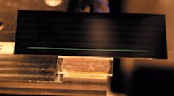
Planar-waveguide optical devices only a couple of centimeters long can combine gratings, thermo-optic phase shifters, Mach-Zehnder WDMs, and other devices in doped-silica waveguide layers deposited onto a silicon chip (see Laser Focus World, Oct. 1999, p. 117). Called a silicon optical bench, such a device can contain V-grooves for passive fiber alignment, laser sources added via hybrid integration, and even an erbium-doped planar optical waveguide amplifier (see Fig. 1).
A group at the University of Twente (Enschede, The Netherlands) is developing planar-waveguide structures based on silicon oxynitride, which has refractive-index tunability over a wide range; clad waveguide channels with a 25-nm core thickness are patterned lithographically into waveguides that transmit well at 1560 nm. Researchers from the Communications Research Center (Ottawa, Ontario, Canada), the Université Laval (Quebec City, Quebec, Canada), and the Center for Research and Education in Optics and Lasers (Orlando, FL) are pursuing the fabrication of integrated optical waveguides in sulfide chalcogenide glasses that have potentially low loss for both the 1300- and 1550-nm telecommunication windows. The material can be processed to include photoinduced Bragg gratings and vertically stacked directional couplers.
Non-WDM-related developments are plentiful. W. L. Gore and Associates (Newark, DE) and Corning combined talents to transmit 10 Gbit/s over 600 m of Corning's 50-µm multimode fiber using Gore's 850-nm vertical-cavity surface-emitting laser (VCSEL). The development of VCSELs for telecommunication and data communication continues, with the devices now the laser source of choice for short-wavelength fiberoptic use (see Laser Focus World, May 1999, p. 235). Researchers at Hitachi (Tokyo, Japan) are developing low-cost plastic optical modules for fiberoptic communications that draw from fabrication techniques developed for integrated circuits, including infrared (IR) die bonding and plastic molded packaging. These are the sorts of practical advances that will help make optical fiber ubiquitous in the office and home.
Not plain old optics
The development of devices based on micro-optoelectromechanical-systems technology proceeds apace. Most well known are the digital micromirror arrays developed by Texas Instruments (Dallas, TX). Already widely commercialized as spatial light modulators used in computer projection displays, they have made their first appearance in movie theaters this year as the projection device for Star Wars: Episode I, The Phantom Menace on two screens in Los Angeles, CA, and two in New York, NY.
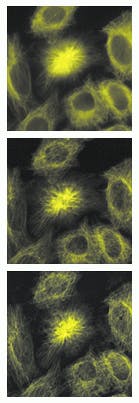
But other MOEMS devices are springing up, some of them based on interesting principles. For example, an uncooled IR camera, developed at the University of California, Berkeley (Berkeley, CA) and Raytheon Systems (Goleta, CA) and intended for low-cost imaging in the 8-14-µm wavelength range, contains an array of tiny interdigitated cantilevered beams that flex when warmed by incident IR radiation, changing their diffraction properties (see Laser Focus World, Nov. 1999, p. 121).A technique being commercialized by CDM Optics (Boulder, CO)—termed "wavefront coding" by the company—combines a cubic phase plate with digital-signal processing to enlarge the focal depth of optical systems by up to a factor of ten, as well as to reduce the effect of lens aberrations (see Laser Focus World, Jan. 1999, p. 28). At first applied to simple optical systems with a low numerical aperture, wavefront coding has now graduated to high-numerical-aperture optics. A 100X oil-immersion microscope objective with a numerical aperture of 1.3, combined with a cubic phase plate, has produced images that have the same degree of sharpness as a confocal scanning microscope over a focal depth of 12 µm when used in fluorescence microscopy (see Fig. 3). Ed Dowski, vice president of CDM, says that the technique not only lowers equipment cost by a factor of two, it also drastically shortens exposure time—an obvious advantage for microscopy. "Biological cells move," he notes.
Light sensors fill needs
Charge-coupled-device (CCD) and CMOS image sensors continue to stake their claims to various portions of the imaging market. With their high fill factor and low noise, CCDs are the high-end leader, while CMOS devices are important at the low end—and, at least in the consumer world, are encroaching upon the middle. Megapixel color CMOS sensors are now available from PixelCam (Campbell, CA), intended for digital still and video-camera use. The largest version has a 1288 x 1032-pixel format with a 7.5-µm-pixel pitch; fill factor is unspecified. Elsewhere, higher-fill-factor active-column CMOS is being pushed by Photon Vision Systems (Cortland, NY), while lower-noise active-pixel format is touted by Photobit (Pasadena, CA); results will come from the marketplace.
Panasonic Security and Digital Imaging (New York, NY) has introduced a CCD camera with a dynamic range increased by a factor of 64. Rather than taking one picture, the Panasonic CCD takes two—the first at a 1/60-s exposure to capture dark areas and the second at a 1/4000-s exposure to capture bright spots—and then combines them electronically, adjusting their gain separately. A series of CCD image sensors introduced by Eastman Kodak (Rochester, NY) has a quantum efficiency of 30% at 400 nm, 50% at 550 nm, and 60% at 650 nm, with array sizes up to 3088 x 2056 pixels.
Common optical-detector materials work poorly or not at all at deep-ultraviolet wavelengths. This is a problem especially for leading-edge optical lithography, which exploits the 248- and 193-nm excimer-laser wavelengths and is moving toward the use of 157 nm. Startech Instruments (New Fairfield, CT) has found a way out by combining ordinary detectors with materials that downconvert deep-ultraviolet radiation to visible light. The choice of downconverter is important, according to Bill Fricke, president, who notes that only certain materials have a linear response. The resulting device detects wavelengths from x-ray to 350 nm, withstands direct laser output without developing color centers, and has a dose sensitivity of 3 x 10⁶ V/J.
About the Author
John Wallace
Senior Technical Editor (1998-2022)
John Wallace was with Laser Focus World for nearly 25 years, retiring in late June 2022. He obtained a bachelor's degree in mechanical engineering and physics at Rutgers University and a master's in optical engineering at the University of Rochester. Before becoming an editor, John worked as an engineer at RCA, Exxon, Eastman Kodak, and GCA Corporation.


