It’s time to focus on photonics manufacturing
RANDY HEYLER
The United States is once again facing a critical turning point in a high-visibility (and potentially highly profitable) technology sector. After successfully developing an enviable lead in photonic-device innovation, we are in danger of following a path that will inevitably yield most of the commercial profits to other countries. The primary reason? We are failing to match the effort to invent with an effort to produce.
The USA is famous for innovation in research and product development, but has a poor record when it comes to manufacturing and profitable commercialization of these ideas. Witness the audio- and video-tape industries—and more recently the compact disk (CD) market, where early innovators in the United States were quickly outpaced—and eventually beaten—by foreign manufacturers whose primary focus was to learn how to economically build the product. Time and again we have seen investment in manufacturing and process technology eventually win out over the initial investments in product or device technology. So why don`t we learn from our previous mistakes?
One problem is the legacy of our high-technology development style. Start-up companies have become ubiquitous, with their potential for realizing quick and substantial wealth creation via the rapid introduction of first-generation ideas and products. Research, design, and product development remain the favored destination for engineers and scientists in this country, while manufacturing remains a second-tier position in many companies, making it difficult to attract or retain top technical talent in process development and production automation. In our high-technology culture, small, quick-strike companies are the norm, the big payouts are to potential profits more often than to demonstrated operating margins, and few companies can muster the financial wherewithal or the long-term interest in building true manufacturing process capability. A secondary effect is the development of products that, while highly innovative, are inherently more costly to produce, eventually limiting pricing flexibility and market penetration.
Compare this to our European and Asian competitors, who have a strong manufacturing legacy and a track record of investing in the plant, equipment, and manufacturing technical personnel required to succeed. Such a legacy creates an atmosphere where products are designed with production in mind, automation is adopted early on, and the focus is to quickly drive down costs and expand market share—all the while steadily incorporating both process and product refinements. Eventually these players build the volume and scale advantages that not only drive others from the market, but can add leverage to their other businesses as well.
Turning manufacturing around
Thankfully, we are starting to see activities here in the USA that bode well for our future. Lucent Technologies (Holmdel, NJ), through its Laser 2000 program, has essentially reinvented the manufacturing process for diode lasers. By following design-for-assembly methods and investing considerably in plant, equipment, and process know-how, Lucent has been able to leverage these developments across all its device production, realizing true low-cost leadership (see Laser Focus World, Dec. 1997, p. 11). Corning Incorporated (Corning, NY) also has recently announced major investments in new plant facilities to deploy new device and fiber manufacturing technologies (see Laser Focus World, April 1997, p. 61). And even some of the newer start-ups, like Lightwave Microsystems (Santa Clara, CA), are leveraging semiconductor manufacturing and process know-how to achieve performance and cost advantages in specialty WDM (wavelength-division multiplexing) products.
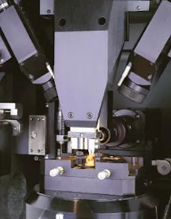
US companies such as Newport Corp. are stepping up their development of assembly, test, and process automation equipment and technology to help photonic-device manufacturers realize true cost savings. These developments are taking the form of sophisticated integrated-process machines that can perform device inspection, testing, characterization, burn-in, assembly, and environmental performance validation—resulting in lower device packaging costs and higher process yields (see photo here and on cover).
Finally, the US government, through NIST and the Ad vanced Technology Program (ATP), is reaching out to US industry to help nucleate the development of next-generation photonics manufacturing techniques, processes, and equipment. The ATP is meant to encourage the formation of consortia to work on the more challenging problems our industry faces in achieving extremely low-cost photonic devices and systems.
The hope is that these activities signal a trend toward a more aggressive manufacturing and process-auto mation strategy here in the United States and a growing respect for the importance of manufacturing and process technology development. This needs to be complemented by an increase in the number of academic programs emphasizing manufacturing and process engineering, design-for-assembly, operations re search, and other production-oriented disciplines, so that US industry can draw from a talent pool conversant in these important technologies. US industry needs to realize the leverage of manufacturing technology to our economic success and create compensation and recognition programs for technical personnel on the factory side that match their counterparts in the R&D department.
Finally, we need to adopt a new production-oriented culture that says, "Making it well is just as important as the invention itself." Only then will we truly realize the commercial profits from our innovations.
