PHOTOVOLTAICS: Quantum dots promise next-generation solar cells
A promising tool for enabling more widespread use of solar energy is the use of nanotechnology to improve the efficiency of a photovoltaic cell’s conversion of energy from visible photons to electrons. In 2001, power-conversion efficiencies of 11% were reported from photoelectrochemical cells constructed from nanocrystalline materials and conducting polymer films.1 Now, researchers at the University of Notre Dame (Notre Dame, IN) have developed a solar cell made from cadmium selenide (CdSe) quantum dots assembled onto titanium dioxide (TiO2) films.2
The use of quantum dots (QDs) in the fabrication of solar cells promises not only high power-conversion efficiencies, but also offers spectral tunability. Because the absorption properties of semiconductor quantum dots are size-dependent, CdSe particles can be tuned from the red to the blue region (from 650 to 400 nm) by decreasing the particle diameter. By assembling the particles in an orderly fashion, the photoresponse of the photovoltaic cell can be tuned, optimizing the spectral response as a function of wavelength.
Multiple charge carriers
Unlike bulk semiconductors, QDs also possess a unique ability to generate multiple pairs of charge carriers with a single high-energy photon. In conventional bulk semiconductors, a single electron-hole pair is generated per absorbed photon. This means that both high- and low-energy photons create only a single pair of charge carriers (electron and hole). More simply, the extra energy of near-UV photons is not utilized fully when using bulk semiconductor films. In QDs, however, high-energy photons can produce multiple charge carriers by a process known as impact ionization, setting the stage to achieve photon-conversion efficiencies greater than 100%.
The researchers used CdSe QDs with diameters of approximately 3 nm (exhibiting band-edge absorption at 550 nm and band-edge emission at 570 nm) and 40- to 50-nm-diameter large-bandgap TiO2 particles that absorb UV light with an onset at 360 nm. The lower-lying conduction band of TiO2 as compared to CdSe minimizes charge recombination and rectifies any charge transport, facilitating interparticle electron transport when the many smaller CdSe QDs are linked to a single TiO2 particle. The linking process, which is necessary to facilitate electron transfer from the QDs, is achieved through a bifunctional linker molecule that contains carboxylate and thiol functional groups that bind CdSe QDs to TiO2.
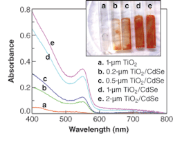
As the thickness of the bound CdSe QDs and TiO2 films increases, the CdSe absorbance increases and the film appears darker (see figure). The increased absorbance is due to the larger number of binding sites available within thicker TiO2 films, which enables increased absorption efficiency for incident photons.
Although the researchers are still far from the goal of achieving photon-conversion efficiencies greater than 100%, their work demonstrates the ability of CdSe QD arrays to harvest photons and generate photocurrent in a photoelectrochemical cell. “Size- and shape-dependent properties of QDs and quantum wires provide a unique opportunity to tailor the properties of photoelectrochemical or photovoltaic cells,” notes Prashant Kamat. “This is the first step in our effort to wire quantum dots with molecular linkers for producing photocurrent. It is our goal to further capitalize on some of these unique properties of QDs and pave the way for developing next-generation solar cells.”
REFERENCES
1. M. Graetzel, Nature 414, 338 (Nov. 15, 2001).
2. I. Robel et al., J. American Chem. Soc. 128, (7) 2385 (January 2006).
About the Author

Gail Overton
Senior Editor (2004-2020)
Gail has more than 30 years of engineering, marketing, product management, and editorial experience in the photonics and optical communications industry. Before joining the staff at Laser Focus World in 2004, she held many product management and product marketing roles in the fiber-optics industry, most notably at Hughes (El Segundo, CA), GTE Labs (Waltham, MA), Corning (Corning, NY), Photon Kinetics (Beaverton, OR), and Newport Corporation (Irvine, CA). During her marketing career, Gail published articles in WDM Solutions and Sensors magazine and traveled internationally to conduct product and sales training. Gail received her BS degree in physics, with an emphasis in optics, from San Diego State University in San Diego, CA in May 1986.