PHOTONIC CRYSTALS: Light moves through tiny hoops at IPRA/Nano
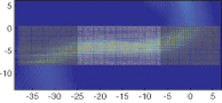
Photonic crystals, silicon photonics, and surface plasmons were all discussed at the OSA topical meetings on Integrated Photonics Research and Applications (IPRA) and Nanophotonics (April 24-28; Uncasville, CT).1 One exciting item in the section on modeling focused on the light-bending capabilities of photonic crystals, in which Kevin Vynck of the University of Montpellier (France) suggested that graded photonic crystals can bend light over short distances with little loss if the rate of change of the gradient is small. His group used iso-frequency curves to design a 2-D graded photonic-crystal device that bends light in an S-shape curve (see figure).
Three methods can be used to gradually change photonic-crystal parameters: changing the lattice spacing so that the holes are spaced farther apart, changing the size of the holes, or gradually changing the refractive index of the material. Bending depends on the wavelength and angle of incidence of the wave, as well as the rate of change of the lattice.
The researchers modeled a three-part graded photonic crystal, in which light from the top right enters the first section and bends in a curve until it is roughly parallel to the surface. The middle section provides a smooth transition to the third (output) section, which again bends the light. Different wavelengths exit the device with different offsets: a 40 nm change in the wavelength (from 1580 to 1540 nm) yields a 7 µm shift at the point at which the beam leaves the device.
The researchers also demonstrated a modeled device that could perform slightly more than a U-turn on 1550 nm light in a distance of 8.5 µm. These devices offer the potential for efficient devices, such as multiplexers, as well as waveguides capable of turning light within a few microns.
Silica on silicon
In another presentation, Lech Wosinski of the Royal Institute of Technology (Kista, Sweden) gave an overview of the use of silicon as a platform for integrated optics.2
In this invited talk, Wosinski described both silica-on-silicon and silicon-on-insulator fabrication technologies, specifically for wavelength-division-multiplexing (WDM) communications. Although silica-on-silicon is a dominant platform for WDM photonics, integrating the silica waveguides with active electronics remains a challenge due to the high temperatures typically used for depositing silica. Wosinski described work at his organization to optimize a low-temperature plasma-enhanced chemical-vapor-deposition (PECVD) process, which has resulted in low-loss germanium-doped silica channels grown on silicon at relatively low temperatures of about 250°C.
His group also used PECVD to deposit amorphous-silicon nanowires that act as waveguides due to their large index-of-refraction contrast. The researchers created a 4 x 4 multiplexer based on an arrayed waveguide grating within a 50 x 50 µm area.
Plasmonics
Waveguiding using surface plasmon-polaritons also provides a way to manipulate light in very small spaces using thin metal coatings. Meir Orenstein of Technion-Israel Institute of Technology (Haifa, Israel), presented experimental results from guiding waves in the dielectric of a deep trench.3 Plasmons are surface-guided waves at the interface between a metal and a dielectric and are usually very short-lived, but in metal strips only a few tens of nanometers thick, plasmons can propagate as far as millimeters. Orenstein’s group demonstrated several novel waveguides.
In slot waveguides, a narrow slot of dielectric (air) separates two 20 nm thick metal layers. In these, the surface plasmons on the sides of the two metal edges of the slot are coupled; two intensity peaks occur at the metal edges. In a trench waveguide, however, the gold layer is much thicker-about 400 nm.
“Here, the dominant plasmonic mode is generated by the tall walls of the trenches-thus it is a really confined mode within the trench and its appearance is a single intensity peak in the middle of the trench,” says Orenstein. “This mode is secured from the surroundings and thus very robust.” These plasmon-based structures could possibly be used to make short-range waveguide devices; if a material were introduced into the slot, it could be used as a very sensitive sensor.
REFERENCES
1. E. Centeno et al., Integrated Photonics Research and Applications/Nanophotonics 2006 Technical Digest (Optical Society of America, Washington, D.C., 2006), NWA4.
2. L. Wosinski Integrated Photonics Research and Applications/Nanophotonics 2006 Technical Digest (OSA, Washington, D.C., 2006), IWA1.
3. Y. Satuby and M. Orenstein, Integrated Photonics Research and Applications/Nanophotonics 2006 Technical Digest (OSA, Washington, D.C., 2006), IWC4.
