High-resolution direct time-of-flight LiDAR brings spatial intelligence to edge AI
Artificial intelligence (AI) is moving out of the cloud and into physical environments, and machines are now being asked to do much more than simply process data. They must perceive, understand, and interact with the real world in real time. Whether navigating a warehouse, monitoring occupancy inside a smart building, assisting healthcare professionals, or enabling gesture-based interaction for augmented reality systems, these applications all depend on one critical capability: Spatial awareness.
For years, time-of-flight (ToF) sensing has powered depth-related applications in consumer electronics—particularly smartphone autofocus and user-interaction systems. But advances in sensor architecture, optics, and edge computing are expanding the technology’s reach. The next phase of ToF extends beyond simply measuring distance by generating AI-ready spatial data to allow machines to understand their surroundings while operating within tight size, power, and cost constraints.
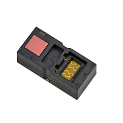
This evolution is seen in direct ToF (dToF) three-dimensional (3D) light detection and ranging (LiDAR) modules, such as STMicroelectronics’ VL53L9 module, which combines high-resolution depth sensing, on-chip processing, and system-level integration within a compact form factor.
From ranging sensor to spatial intelligence engine
Traditional ToF systems have historically been used for single-point ranging or relatively low-resolution depth measurements. While effective for proximity sensing, these architectures offered limited environmental understanding and are therefore best suited to simple use cases.
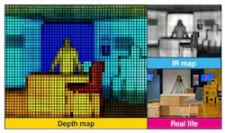
The emergence of high-resolution multizone dToF sensors changes this equation. Instead of providing a single distance measurement, modern LiDAR modules generate detailed depth maps of an entire scene. Our dToF module, for example, provides 54 × 42 sensing zones—2,268 independent depth points—while maintaining frame rates up to 100 fps and a sensing range extending from less than 5 cm to 9 m.
This combination of spatial resolution, speed, and range enables a level of environmental understanding previously associated with significantly larger and more expensive systems. Detecting and tracking small objects, edges, contours, and moving targets with high accuracy opens new opportunities in robotics, industrial automation, smart buildings, healthcare monitoring, and consumer electronics.
Direct ToF matters
Unlike indirect ToF approaches that infer distance through phase measurements, dToF directly measures photon travel time. This provides greater robustness across a wide range of operating conditions and enables highly accurate ranging performance.
The receiver circuitry of the latest dToF systems contains an array of single-photon avalanche diodes (SPADs), which are capable of detecting individual photons with exceptional sensitivity. Advances in stacked backside-illuminated (BSI) SPAD architectures are allowing manufacturers to dramatically increase sensor resolution and maintain compact dimensions and low power consumption.
Our system leverages a proprietary stacked BSI SPAD design combined with metasurface optics to enable accurate ranging with up to 1% accuracy while achieving a wide 54° × 42° field of view within a module measuring only 12.8 mm × 6.1 mm × 4.6 mm.
Beyond depth: Combining infrared and 3D data
One of the more significant developments in modern ToF systems is the shift from pure depth sensing toward multimodal perception.
Beyond generating basic range information, advanced LiDAR modules can simultaneously provide multiple data streams, including depth maps, infrared (IR) imagery, reflectance information, ambient light measurements, and confidence metrics.
Our dToF module, for example, produces both 3D depth information and complementary IR imaging. This combination is particularly valuable for AI applications because it provides structural information about a scene and preserves computational efficiency. Unlike RGB cameras, which often require substantial AI processing, depth and IR outputs can simplify object segmentation, motion analysis, and environmental understanding.
Privacy preservation is another benefit. Because ToF systems measure geometry rather than identifying visual details, applications such as occupancy monitoring, people counting, posture analysis, and presence detection can be implemented without capturing recognizable personal images.
Rethinking illumination architecture
The design of the illumination subsystem in the transmitter part of the module remains a critical element of LiDAR performance.
Many traditional ranging systems rely on dot-projector architectures that sequentially scan portions of a scene. While effective in some applications, these approaches can introduce blind spots, motion artifacts, and limitations when tracking fast-moving objects.
Newer architectures are increasingly adopting flood-illumination techniques. Our dToF modules use a dual-scan flood illumination system using two dual-junction vertical-cavity surface-emitting laser (VCSEL) emitters that illuminate the entire scene simultaneously. This approach improves small-object detection, reduces motion artifacts, eliminates dead zones, and captures complementary IR and depth imagery from the same scene. The result is cleaner, more complete spatial data that can be processed efficiently at the edge.
Enabling edge AI
Among the most powerful trends shaping the future of optical sensing is the migration of AI inference toward embedded systems.
Many industrial and consumer applications can’t rely on cloud connectivity due to latency, privacy, bandwidth, or power limitations. Instead, sensing systems increasingly need to perform analytics locally using microcontrollers or power-constrained processors. This creates a strong incentive for sensors to become more intelligent and deliver structured information rather than raw data. Modern LiDAR modules increasingly incorporate on-chip processing capable of generating AI-ready outputs directly from the sensor.
In demonstration systems based on an STM32H5 microcontroller, analytics powered by the VL53L9 ran at 30 fps and consumed only a fraction of available memory resources—making sophisticated perception workloads feasible on compact embedded platforms. Applications demonstrated include safety-zone monitoring, advanced people sensing, fall detection, posture tracking, and gesture recognition.
Expanding use cases
The combination of high-resolution depth sensing, compact integration, and low compute requirements enables deployment across a broad range of industries.
For robotics, precise depth maps support simultaneous localization and mapping (SLAM), obstacle avoidance, and navigation. Industrial systems can leverage the technology for volume measurement, inventory monitoring, and machine safety. Smart buildings gain occupancy analytics and people-flow monitoring while preserving privacy. Healthcare applications include fall detection and patient monitoring, while AR/VR systems benefit from gesture recognition, body tracking, and finger skeleton tracking.
Future of machine perception
The broader significance of high-resolution dToF LiDAR extends beyond any single application. It reflects a larger industry transition from imaging intended for human interpretation toward sensing designed for machine perception.
As AI systems become increasingly embedded in factories, buildings, robots, healthcare devices, and consumer products, sensors must deliver meaningful contextual information rather than simply collect data. Depth, IR sensing, embedded intelligence, and system-level integration are converging to create perception platforms capable of transforming light into trusted data.
High-resolution dToF LiDAR is emerging as one of the foundational technologies enabling this transition—bringing robust spatial intelligence to edge devices that must see, understand, and act in the real world.
About the Author
 Laurent Plaza
Laurent Plaza
Laurent Plaza is the Time-of-Flight & Ambient Light Sensing product line manager for STMicroelectronics. He has more than 25 years’ experience in the semiconductor industry, combining technical, product, and commercial expertise to turn innovation into successful products and business growth, with more than 3 billion ToF units shipped to date.