Optical spectroscopy enables next-gen semiconductors
In the race to develop more efficient electronics, it’s critical to understand materials at an atomic scale. Optical spectroscopy, a noninvasive technique that uses light to characterize materials, is undeniably one of the cornerstones advancing semiconductor research. From Raman spectroscopy to ellipsometry, these techniques allow researchers to explore semiconductor materials with extraordinary precision.
Semiconductor development
Raman spectroscopy is particularly effective for measuring the crystallinity of semiconductor materials, such as silicon carbide (SiC), copper indium gallium diselenide (CIGS), and cadmium telluride (CdTe). It relies on the inelastic scattering of photons by molecules, which happens when incident light interacts with lattice vibrations within the material and causes a measurable energy shift known as the Raman shift. This shift can be used as a spectral fingerprint, which makes it possible to identify crystal phases, defects, and stress within semiconductor structures—all of which are important to optimize electronic performance and fabrication processes.
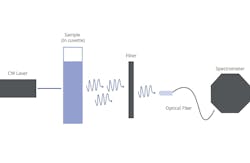
Photoluminescence spectroscopy is based on shining light of a specific wavelength onto a material, which causes the electrons within it to be excited to a higher energy level. When they relax back to their lower energy states, they emit light that can be detected by a spectrometer (see Fig. 1). Analyzing the spectra that is produced can provide information about the material, but for semiconductor materials research it is used to assess the material’s composition and to check for defects. Within crystalline materials, such as SiC, this data is specific enough to determine the internal stresses of crystal defects.
Since the 1960s, ellipsometry has developed to a point where it provides the sensitivity necessary to measure nanometer-scale layers used within microelectronics. It works by directing polarized light toward a material, and then measuring the way the polarization is affected after the light interacts with the material. These changes are compared to a model of the sample to work out information about the material, such as its optical properties and thickness. Unsurprisingly, it is primarily used to determine film thickness and optical constants. But it can also be used to characterize material composition, doping concentration, and crystallinity.
Impact on emerging semiconductor technologies
Optical spectroscopy is an important tool to develop new semiconductor technologies in which precision and performance are critical. One of the biggest areas that requires a rapid improvement in semiconductor technology is artificial intelligence (AI). In fact, the global semiconductor market is expected to grow by 15% in 2025 alone,1 largely due to AI’s influence. As AI continues to become more accessible and commonplace within our day-to-day lives, semiconductors need to be further optimized for speed, thermal stability, and low power consumption to keep up with the huge computational power demands.
Raman spectroscopy and ellipsometry are making this possible, because they enable the precise assessment of key material properties such as strain and uniformity at advanced technology nodes. These characteristics have a direct influence on transistor switching speeds and heat dissipation, both of which are important for creating high-performance AI chips. To complement these optical techniques, probe stations and other high-precision characterization tools like micromanipulators2 can be used along with spectroscopy to correlate electrical performance with material characteristics during device fabrication.
Semiconductors are also central to the growing quantum computing industry where they are required to create qubits (basic unit of quantum information). Unlike classical bits, which exist as either 0 or 1, qubits can exist in multiple states simultaneously. This property enables quantum computers to perform many calculations at once, which allows them to solve problems that are beyond the reach of traditional systems.
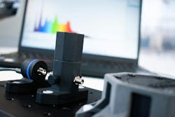
The semiconductor materials used for quantum computing require highly controlled quantum states. One such material is quantum dots, which are nanoscale semiconductor particles. Quantum computing systems are extremely sensitive to imperfections down to the atomic scale, and can be assessed via optical spectroscopy. Photoluminescence spectroscopy, for example, makes it possible to probe exciton behavior and defect states, which can affect coherence times and qubit fidelity. Raman spectroscopy is capable of identifying photon interactions that can lead to decoherence. These tools are therefore essential for performing quality control by screening materials used in quantum devices (see Fig. 2).
Optical spectroscopy also enables the development of new materials for next-generation semiconductors, particularly two-dimensional (2D) materials. These are crystalline substances made of a single layer of atoms, which gives them unique electrical, optical, and mechanical properties. Interest in 2D materials took off in 2004 with the isolation of graphene, a single layer of carbon atoms known for its exceptional conductivity and strength.
Since then, the field has grown rapidly and materials like molybdenum disulfide (MoS2) and tungsten disulfide (WS2) showing great potential3 for applications within ultrathin transistors. Thanks to their atomic-scale thickness and tunable properties, 2D materials are strong contenders in the race to create smaller, more efficient semiconductor devices. Optical spectroscopy techniques are key to their development. Raman spectroscopy is commonly used to identify the number of layers within the material and detect defects, while ellipsometry can confirm thickness measurements and assess the uniformity of the 2D films.
Future directions
Overall, as semiconductor research continues to evolve, optical spectroscopy will remain an essential tool by providing the precision needed to design and scale the materials and devices of the future. Continued advances in our current optical spectroscopy techniques need to focus on improving the spatial, temporal, and spectral resolution to make easier nanoscale characterization a reality. Integrating these techniques with machine learning and enabling in situ measurement capabilities to make real-time process monitoring possible will help shape the future of semiconductor development.
REFERENCES
About the Author
Caitlin Ryan
Caitlin Ryan is a Ph.D. student in materials science and scientific writer at Ossila, a U.K.-based company that specializes in lab equipment and advanced materials used for solar cell and semiconductor research, driving the development of high-efficiency photovoltaics, flexible OLED screens, next-generation semiconductors, and more. She holds an MEng degree from the University of Leeds, U.K.

