Integrated solutions key to fast, accurate, and repeatable PIC testing
Photonic integrated circuit (PIC) technology is emerging as a key driver of high-speed networks and 5G mobility, largely due to vastly accelerated development of transceivers and passive components that are smaller, faster, cheaper, and greener than their bulk optics counterparts. With the help of process design kits (PDKs), PIC designs are no longer limited to the conventional versions found in the legacy telecom components portfolio. Designs of entirely new components even enable expansion beyond the borders of telecom into applications found in the lidar, medical, and sensing industries. Testing these new PIC designs poses challenges not previously encountered, requiring various types of manufacturing and test instrumentation to work together flawlessly in innovative ways. At the same time, the test technology must remain scalable and future-proof to minimize capital expenditure (CAPEX).
PIC testing objectives for compliance benchmarks
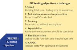
The six PIC testing objectives shown in Figure 1 are the most common benchmarks when deciding what instrumentation to choose for manufacturing and characterizing the PIC under test. The speed of testing is the first objective and must be considered in the context of item 6—CAPEX—as it comprises the bulk of component manufacturing costs. The speed of characterization is not limited to the test instrumentation used. It also includes the alignment of the optical and/or electrical probes to and from the PIC under test (see Fig. 2).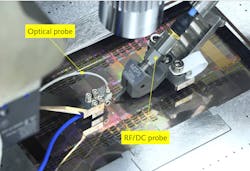
The first major challenge to speedy testing is that the alignment of the probes onto the PIC requires a wafer disc probe handler, which must be capable of interfacing with the test instrumentation responsible for characterization of the device. This is typically insertion loss, return loss, and/or polarization-dependent loss (PDL), all as a function of wavelength. In the case of a hybrid PIC, this would not be limited to power supply settings or current readings as a function of wavelength.
Finding the optimum alignment positions of the optical and/or electrical probes in and out of the PIC is a challenge and is a critical part of keeping the total testing time to a bare minimum. There are proven, fully automated geo-mapping techniques capable of finding the optimum position within a fraction of a second, utilized by the connected test instrumentation as a trigger to start taking measurements.
Test and measurement response time. This is not to be underestimated, as it requires the response time of the test instrumentation involved to respond faster than the PIC under test. This can be particularly challenging when testing passive PIC components with sharp roll-off values such as ring resonators (see Fig. 3). Such applications may require measurements to be taken at reduced scanning speeds at the expense of longer measurement times, subsequently incurring higher costs.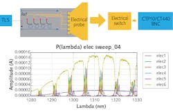
Measurement accuracy and repeatability. These objectives are interrelated and directly responsible for the total time required to complete the PIC characterization. Running measurements multiple times to ensure accurate and repeatable measurement results is costly and inefficient. Optical test instrumentation based on Michelson interferometry synchronization with absolute wavelength reference standards—such as acetylene gas cells and full dynamic range optical power meters—address these to the maximum extent possible.
Addressing flexibility, scalability, and CAPEX. These considerations are the easiest to address from an integration perspective, as they make use of modular-type test solutions and platforms. Having a base system in place allows the addition of features and functions over time without initial investments; it could also allow for integrated optical and electrical parameter testing.
Key to optimizing PIC testing: collaboration
Since no one company makes all items required to build and test PICs, the manufacturer must find solutions that enable integration of test instruments from multiple vendors into one automated test setup. The aforementioned objectives can serve as compliance benchmarks.
For example, to support PIC manufacturers striving to achieve the optimum result and deliver integrated test solutions, EXFO (Québec City, QC, Canada) has collaborated with other equipment vendors—MPI Corporation (Chu-pei City, Taiwan), addressing the wafer disc handler aspects, and the Hewlett-Packard Enterprises (HPE; Palo Alto, CA) for PIC design (see Fig. 4). EXFO has also worked with Maple Leaf Photonics (Seattle, WA) to tackle system integration and software automation as well as custom wafer disc handler systems.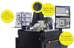
Collaboration beneficiaries
Two use cases that have experienced immediate benefits from vendor collaborations are Tower Semiconductor (Migdal HaEmek, Israel) and AEPONYX (Montréal, QC, Canada).
Tower Semiconductor’s activities are foundry-based. Dealing with a large customer base leaves no room for questionable measurement results. It requires data to be traceable throughout the PIC ecosystem chain, from design to finished product.
Every customer and PIC device are subject to a different test setup, so scalability and customization are critical. Tower Semiconductor chose the collaborative solution of EXFO’s CTP10 passive optical component test system with the MPI TS3000 wafer disc handler system to meet its needs.
AEPONYX, a PIC inventor and micro-optical switch manufacturer creating chips for fiber-optic access to the cloud, needed to find a solution for faster test processing of its advanced silicon photonics devices that combine silicon photonics, MEMS-based switches, and waveguides in one device. Combining silicon nitride waveguide photonics and planar MEMS on a single chip presented a unique challenge because the test solution needed to cover both optical and electrical probing. High-volume production demanded a solution that could test hundreds of thousands of devices for use in both development and production stages.
Specifically, this included a fully automated optoelectrical probing system with ultrafast optical test instrumentation capable of generating the large set of data needed for device characterization. AEPONYX, armed with the challenge of designing a fully integrated test solution, reached out to EXFO and Maple Leaf Photonics. This collaboration addressed the requirement for a solution with customized firmware, enabling autonomous device-to-device displacement and locking based on optical signal quality. The result was a fully automated measurement system that dramatically increased the testing speed by a factor of 10 compared to previous technologies.
With exponential growth demand for PIC testing, component manufacturers will increasingly need innovative and collaborative solutions that are scalable, future-proof, and cost-effective to optimize testing processes.
About the Author

Lawrence van der Vegt
Lawrence van der Vegt is the head of photonics at MPI Corp. He is an optics veteran; he earned his bachelor's degree in electrical and computer engineering at De Blauwe Kei College (Netherlands) and has held various key directorial positions at optical test and measurement companies in The Netherlands and the U.S.