NIST uses terahertz waves to make ultrasensitive silicon measurements

Feb. 28, 2020
National Institute of Standards and Technology (NIST) scientists have made the most sensitive measurements to date of silicon’s conductivity in order to improve future solar cell and semiconductor applications.
Sean Kelley/NIST
To create electric charges in silicon, researchers shine pulsed laser light onto a sample. One-photon tests using visible light only penetrate a tiny way into a silicon sample--on the order of micrometers or smaller. But the new two-photon tests using near-infrared light penetrate much, much deeper into silicon--on the order of millimeters or longer. The one-photon tests create a lot of electric charge (shown here as pluses and minuses) in a relatively small volume. By contrast, the two-photon test creates far fewer electric charges in a much larger volume.

Silicon, the best-known semiconductor, is ubiquitous in electronic devices including cellphones, laptops and the electronics in cars. Now, researchers at the National Institute of Standards and Technology (NIST) have made the most sensitive measurements to date of how quickly electric charge moves in silicon, a gauge of its performance as a semiconductor. Using a novel method, they have discovered how silicon performs under circumstances beyond anything scientists could test before--specifically, at ultralow levels of electric charge. The new results may suggest ways to further improve semiconductor materials and their applications, including solar cells and next-generation high-speed cellular networks. The NIST scientists detail their terahertz spectroscopy technique in Optics Express.

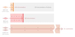
Unlike previous techniques, the new method does not require physical contact with the silicon sample and allows researchers to easily test relatively thick specimens, which enable the most accurate measurements of semiconductor properties.

The NIST researchers had previously done a proof-of-principle test of this method using other semiconductors. But this latest study is the first time researchers have pitted the new light-based technique against the conventional contact-based method for silicon.

It’s too soon to say exactly how this work might be used someday by industry. But the new findings could be a foundation for future work focused on making better semiconducting materials for a variety of applications, including potentially improving efficiency in solar cells, single-photon light detectors, LEDs, and more. For example, the NIST team’s ultrafast measurements are well-suited to tests of high-speed nanoscale electronics such as those used in fifth-generation (5G) wireless technology, the newest digital cellular networks. In addition, the low-intensity pulsed light used in this study simulates the kind of low-intensity light a solar cell would receive from the Sun.

When researchers want to determine how well a material will perform as a semiconductor, they assess its conductivity. One way to gauge conductivity is by measuring its “charge carrier mobility,” the term for how quickly electric charges move around within a material. Negative charge carriers are electrons; positive carriers are referred to as “holes” and are places where an electron is missing.

The conventional technique for testing charge carrier mobility is called the Hall method. This involves soldering contacts onto the sample and passing electricity through those contacts in a magnetic field. But this contact-based method has drawbacks: The results can be skewed by surface impurities or defects, or even problems with the contacts themselves.

To get around these challenges, NIST researchers have been experimenting with a method that uses terahertz (THz) radiation.

NIST’s THz measurement method is a rapid, noncontact way to measure conductivity that relies on two kinds of light. First, ultrashort pulses of visible light create freely moving electrons and holes within a sample--a process called “photodoping” the silicon. Then, THz pulses, with wavelengths much longer than the human eye can see, in the far infrared to microwave range, shine on the sample.

Unlike visible light, THz light can penetrate even opaque materials such as silicon semiconductor samples. How much of that light penetrates or is absorbed by the sample depends on how many charge carriers are freely moving. The more freely moving charge carriers, the higher the material’s conductivity.

For the full story, see the source link below.

SOURCE: NIST; https://www.nist.gov/news-events/news/2020/02/how-low-can-you-go-lower-ever

About the Author

Gail Overton | Senior Editor (2004-2020)

Gail has more than 30 years of engineering, marketing, product management, and editorial experience in the photonics and optical communications industry. Before joining the staff at Laser Focus World in 2004, she held many product management and product marketing roles in the fiber-optics industry, most notably at Hughes (El Segundo, CA), GTE Labs (Waltham, MA), Corning (Corning, NY), Photon Kinetics (Beaverton, OR), and Newport Corporation (Irvine, CA). During her marketing career, Gail published articles in WDM Solutions and Sensors magazine and traveled internationally to conduct product and sales training. Gail received her BS degree in physics, with an emphasis in optics, from San Diego State University in San Diego, CA in May 1986.

Sponsored Recommendations

How Precision Motion Systems are Shaping the Future of Semiconductor Manufacturing

March 28, 2024
This article highlights the pivotal role precision motion systems play in supporting the latest semiconductor manufacturing trends.

Understanding 3D Printing Tolerances: A Guide to Achieving Precision in Additive Manufacturing

March 28, 2024
In the world of additive manufacturing, precision is paramount. One crucial aspect of ensuring precision in 3D printing is understanding tolerances. In this article, we’ll explore...

Automation Technologies to Scale PIC Testing from Lab to Fab

March 28, 2024
This webinar will cover the basics of precision motion systems for PIC testing and discuss the ways motion solutions can be specifically designed to address the production-scale...

Case Study: Medical Tube Laser Processing

March 28, 2024
To enhance their cardiovascular stent’s precision, optimize throughput and elevate part quality, a renowned manufacturer of medical products embarked on a mission to fabricate...

Voice your opinion!

To join the conversation, and become an exclusive member of Laser Focus World, create an account today!