Light measures nanoscale features
Incorporating news from O plus E magazine, Tokyo
TOKYONABA Corp., in collaboration with Nano Focus (Duisburg, Germany) and others, has developed and begun to market three different nanoscale three-dimensional (3-D) surface measurement systems. The precision of the devices reaches 3.4 nm with a measurement range up to 180 mm. All the devices use light and so do not contact the surface directly. Therefore, unlike scanning electron microscopy (SEM), these instruments do not damage the object. In addition, actual measurements of height and width can be made, so detailed modeling of 3-D surfaces can be performed.
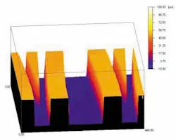
The three instruments are based on different mechanisms, and the appropriate mechanism can be chosen depending on the desired precision and measurement range. One version can be used for microelectromechanical systems (MEMS) products such as injection molds for MEMS optical switches, for example, another can be used for surface mounted products such as integrated-circuit components, and a third can be used for metallic products (see figure).
Noncontact nanoscale measurement system measures topography of features intended for use in microelectromechanical systems (top). The measurement system itself fits on a small stand (bottom).
All the systems are compact. A separate monitor displays the measurement range, so the range can be checked frequently, reducing setup time. The programming language Visual Basic can be used to easily build an automatic measurement program.
Because these are noncontact systems, they are useful for both research and development work or on the production line without interfering with the next process. It is unnecessary, therefore, to produce many samples for testing. In addition, the measurement speed is 100 times faster than that of a SEM, so testing time can be greatly reduced. By combining these devices with 3-D computer-aided design, the design and development processes can be greatly streamlined.
Courtesy O plus E magazine, Tokyo


